

- 中文
- English
- Español
Two Japanese universities jointly announced that diamond + gallium nitride improves heat dissipation performance by 2.3 times!
2023-12-29 09:39:54
Click:
“
With the continuous development of science and technology, the functions of electronic devices are becoming more and more powerful, but at the same time, it also brings heat dissipation problems. Traditional heat dissipation materials can no longer meet the needs of modern electronic equipment. Therefore, finding new heat dissipation materials has become an important issue in the field of science and technology.
”
With the continuous development of science and technology, the functions of electronic devices are becoming more and more powerful, but at the same time, it also brings heat dissipation problems. Traditional heat dissipation materials can no longer meet the needs of modern electronic equipment. Therefore, finding new heat dissipation materials has become an important issue in the field of science and technology.
Recently, Japan's Osaka Public University (OMU) and Japan's Tohoku University Institute of Metal Materials jointly announced that they used diamond, which has the highest thermal conductivity among all materials, as a substrate and successfully manufactured gallium nitride transistors on diamond. , the heat dissipation performance is improved by 2.3 times compared to the same shape transistor fabricated on a silicon carbide (SiC) substrate.

Both diamond and gallium nitride are materials with high thermal conductivity. Diamond is the substance with the highest thermal conductivity in nature, while gallium nitride is one of the substances with the highest thermal conductivity among synthetic compounds. Combining these two materials can fully exploit their advantages and achieve more efficient heat dissipation.
So, how does diamond + gallium nitride achieve efficient heat dissipation?
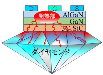
First, both diamond and gallium nitride have extremely high thermal conductivities. The thermal conductivity of diamond is as high as 2000W/m·K, while the thermal conductivity of gallium nitride has also reached 300W/m·K. This means they can quickly transfer heat to their surroundings, avoiding the problem of heat building up inside the material.
Secondly, the combination of diamond and gallium nitride also helps improve heat dissipation performance. Coating a gallium nitride film on the diamond surface can increase the heat transfer path and improve heat dissipation efficiency. In addition, the bonding force between diamond and gallium nitride is very strong, which can effectively prevent heat loss at the interface.
In this study, the research team first produced a 3 μm thick gallium nitride layer and a 1 μm thick 3C-SiC buffer layer (3C-SiC, a type of cubic crystal system) on a silicon substrate. The two layers were then peeled off from the silicon substrate and bonded to a diamond substrate using a "surface-active bonding method," resulting in a gallium nitride transistor with a size of about 1 inch (2.5 cm). According to the research team, due to the use of high-quality silicon carbide films, even if heat treatment is performed at a high temperature of 1100°C, there will be no film delamination on the junction interface, thus obtaining a high-quality heterojunction interface.
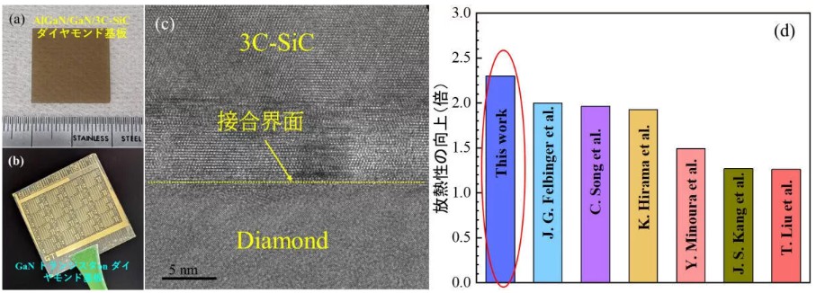
Next, the research team compared the heat dissipation of gallium nitride transistors fabricated on a diamond substrate with the same shape of transistors fabricated on a silicon carbide substrate. The results confirmed that transistors on diamond substrates had approximately 2.3 times greater heat dissipation capacity than transistors on silicon carbide substrates. In addition, their experimental transistors on diamond substrates achieved better heat dissipation than transistors fabricated on diamond substrates in other previous studies, and the characteristics of the transistors were also significantly improved.
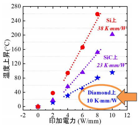
This research significantly improves the heat dissipation and maximum power output of GaN power devices. This will help reduce system size, simplify cooling mechanisms, and significantly reduce energy consumption. The research team stated that this new combination of heat dissipation materials has broad application prospects. In the future, using diamond substrates to realize large-area gallium nitride transistors is expected to expand the application of high-power semiconductor components in 5G communication base stations, weather radar, satellite communications and other fields. scope. In addition, due to its efficient heat dissipation properties, diamond + gallium nitride can also be used to create smaller, lighter, and more reliable electronic devices. With the continuous advancement of technology, it is believed that this new combination of heat dissipation materials will play an increasingly important role in the future.
As a semiconductor diamond production supplier, High Light Intelligence Technology is developing rapidly in the semiconductor industry. We also provide diamond materials to major commercial customers and academic researchers, contributing to the development of semiconductor technology and materials.With MPCVD technology as the core, we have long been committed to the R&D and manufacturing of high-quality diamond materials and related equipment. We have advanced MPCVD equipment, laser processing equipment and precision polishing equipment.









-

CVD Single-Crystal Diamonds: An Analysis of the Complete Processing Workflow from Gas-Phase Deposition to Finished Diamond Chips
MPCVD (Microwave Plasma Chemical Vapor Deposition) technology is currently the core process for producing high-quality single-crystal diamond s. Thanks to its advantages of low defect rates, high purity, and controllable large dimensions, it is widely used in fields such as semiconductor heat dissipation, precision optics, and high-end sensors. The final quality of single-crystal diamond s depends on comprehensive process control throughout the entire workflow—from vapor deposition growth to pos
-
Single-Crystal or Polycrystalline Diamond — Which Has Greater Potential?
As diamond continues to enter industries such as semiconductors, thermal management, optics, high-power electronics, and precision machining, the requirements for diamond materials are also evolving.
-
Diamond Polishing and Grinding Processes: Core Challenges and Industry Hurdles
Diamond is often hailed as the “ultimate material” – ranking 10 on the Mohs hardness scale, boasting an ultra‑high thermal conductivity (~2,200 W/(m·K)), excellent chemical stability, and broad optical transparency. These properties make it irreplaceable in cutting‑edge applications such as semiconductor heat dissipation, high‑end optics, and quantum chips. Yet the paradox of “good materials are hard to process” is nowhere more evident than in diamond. From rough grinding for planarization to at
-
Single-Crystal vs Polycrystalline CVD Diamond: Process Difference Lies in Growth Logic, Not Equipment
The process difference between single crystal and polycrystalline CVD diamond lies not in equipment, but in growth logic. Single crystal and polycrystalline CVD diamond are two functional new materials with completely independent growth mechanisms, lattice structures and performance systems. Their process logic, product features and application boundaries diverge fundamentally from the very start of deposition and growth. Comparing or selecting materials without considering their underlying crys




