

- 中文
- English
- Español
The new results of the team of Academician Tian Yongjun of Yanshan University are published in Nature again: room temperature structural transformation and migration of diamond interface
2024-01-16 09:01:38
Click:
“
On January 4, 2024, Beijing time, Nature magazine published online the latest results of the team of Academician Tian Yongjun of the High Voltage Science Center of the State Key Laboratory of Metastable Materials Preparation Technology and Science at Yanshan University. Researchers systematically characterized multiple atomic-level configurations coexisting on Σ3{112}/<110>incoherent twin boundaries in nanotwinned diamond and recorded in situ the dislocation-mediated interface at room temp
”

In nanotwin materials with face-centered cubic structure or diamond structure, Σ3{112}/<110>incoherent twin boundary (ITB) is a common interface. In metals, this interface will migrate rapidly when the twin thickness is lower than a certain critical value, inducing the detwinization process, which is also the key reason for the softening of metal materials with nanotwin structures. Unlike metal materials, nanotwinned cubic boron nitride and nanotwinned diamond do not soften as the twins are further refined, and the hardness of the materials continues to increase. This shows that Σ3{112} ITB has high stability in covalent materials that is very different from that of metal systems. Exploring the structural origin of this high stability is of great significance for understanding the continuous hardening mechanism of nanotwinned diamond and developing high-performance nanotwinned structural materials.
This research work was supported by the National Natural Science Foundation, the National Key Research and Development Program, the Hebei Provincial Natural Science Foundation and other projects.
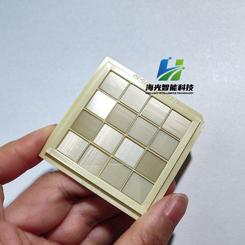
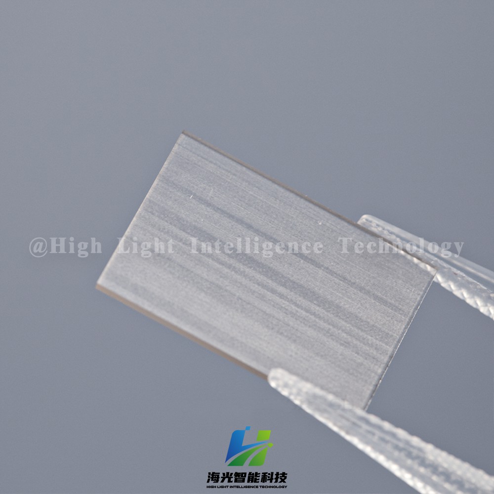
As a semiconductor diamond production supplier, High Light Intelligence Technology is developing rapidly in the semiconductor industry. We also provide diamond materials to major commercial customers and academic researchers, contributing to the development of semiconductor technology and materials.With MPCVD technology as the core, we have long been committed to the R&D and manufacturing of high-quality diamond materials and related equipment. We have advanced MPCVD equipment, laser processing equipment and precision polishing equipment.


-
Z-Axis System: The Key to Stable Production of MPCVD Diamonds
Microwave Plasma Chemical Vapor Deposition is the mainstream method for producing high-quality diamonds in the industry. When the equipment is running, it first pumps the reaction chamber into a vacuum state to strictly ensure the chamber is fully sealed and airtight. Then, the microwave device releases energy, and special mixed reaction gases are fed into the chamber. Under the action of energy, a stable plasma area is formed. These highly active plasmas provide stable heat and reaction conditi
-
How to Choose the Right MPCVD Equipment?
MPCVD equipment is a critical asset across a wide range of industries, including industrial manufacturing, semiconductor thermal management, precision cutting tools, and lab-grown diamonds. Choosing the right equipment not only boosts production efficiency and ensures consistent product quality but also effectively controls long-term costs, making your entire production process smoother and more competitive. Many people struggle with the question: How do I make the right choice? Today, drawing o
-
CVD Diamond Clarity: How to Avoid Inclusions That Affect Jewelry Value
After selecting a loose diamond, the setting not only determines the diamond’s security but also directly affects its perceived size. With diamonds of the same weight, choosing the right setting design can effortlessly create the surprise of “small carats making a big impact,” saving on your budget while enhancing the diamond’s quality. Among these, pavé and prong settings are the two most classic and effective ways to make a diamond appear larger. Paired with specialized designs that maximize t
-
How Diamond Became the Ultimate Thermal Solution in the Era of Computing Power
The iconic narrative behind the legendary "A Diamond is Forever" slogan has long been upended by China's industrial prowess. Once synonymous with luxury and rarity, this gem has shed its glamorous aura to become an indispensable thermal management material for high-power devices. In an era of explosive growth in AI computing power, it has taken up the mantle of "cooling to save computing power".


