

- 中文
- English
- Español
The Zhengzhou Research Institute of Harbin Institute of Technology has made important progress in the field of preparing pure and dispersed nanodiamonds by CVD method.
2024-03-15 09:28:34
Click:
“
Nanodiamond (ND) is mainly obtained through detonation or high pressure and high temperature (HPHT) methods. They are often surrounded by a non-diamond shell, resulting in emission quenching and color center instability. Furthermore, functional groups on the particle surface containing oxygen and nitrogen lead to hard agglomeration. ND can be obtained after high temperature and high pressure diamond crushing. They have sharp edges that will scratch the surface and contain metal impurities in the
”
Nanodiamond (ND) is mainly obtained through detonation or high pressure and high temperature (HPHT) methods. They are often surrounded by a non-diamond shell, resulting in emission quenching and color center instability. Furthermore, functional groups on the particle surface containing oxygen and nitrogen lead to hard agglomeration. ND can be obtained after high temperature and high pressure diamond crushing. They have sharp edges that will scratch the surface and contain metal impurities in the working environment. Both techniques are time-consuming. Other methods for preparing ND include high-energy ball milling, laser shock wave, etc
Generally, CVD-prepared NDs are nucleated directly on the substrate or seed substrate, and the nucleation and growth processes occur continuously in the growth environment, resulting in easy formation of interconnections between particles. Considering the independent particles, growth must be stopped before they come into contact, which will result in low yields. Additionally, the particles are difficult to collect due to their strong adhesion to the substrate. Due to the limitations of these methods, new preparation methods must be developed. In a microwave plasma-assisted chemical vapor deposition (MPCVD) growth environment, diamond may be able to nucleate in the gas phase. However, the nucleation environment and growth mechanisms have not been further studied.
Recently, the infrared thin film and crystal team of Harbin Institute of Technology used microwave plasma-assisted chemical vapor deposition (MPCVD) technology to perform gas-phase nucleation by regulating the plasma state. The prepared NDs have high dispersion, high purity, good shape controllability, and defect-free properties. The advantages of low density have greatly promoted the application competitiveness of NDs in high-precision application fields. Relevant research results were published in "Powder Technology" under the title "Vapor phase nucleation and sedimentation of dispersed nanodiamonds by MPCVD" and obtained a Chinese invention patent.
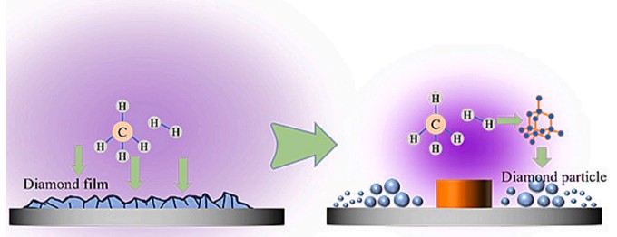
Image and text guide
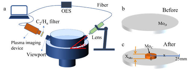
Figure 1. (a) Schematic diagram of the OES and filter observation method for measuring plasma; (b) Schematic diagram of the molybdenum tray; (c) Relative position of the molybdenum tray and the molybdenum column.
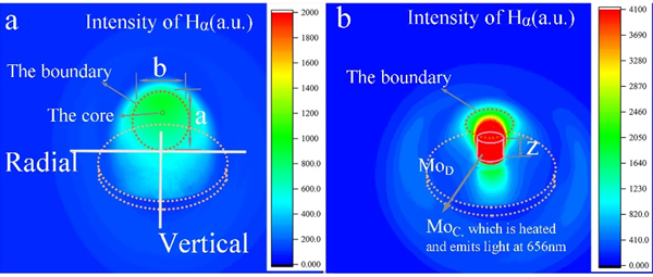
Figure 2. (a) Spatial distribution of Hα when MoC is not used (b) Spatial distribution of Hα when MoC is used
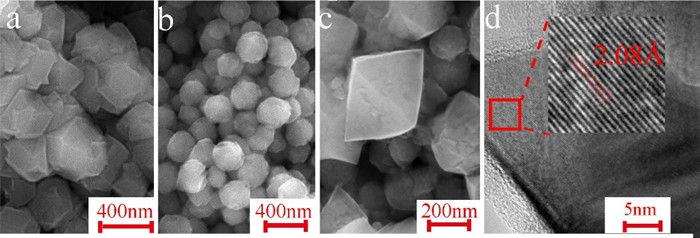
Figure 3. (a) SEM of NDs prepared without MoC; (b-d) SEM&TEM of NDs prepared with MoC
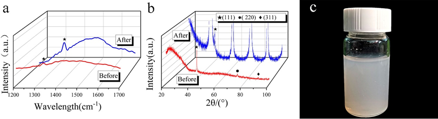
Figure 4. (a) Raman spectrum of nanodiamond before and after using MoC; (b) XRD pattern of nanodiamond before and after using MoC; (c) Nanodiamond dispersion
Application prospects
At present, nanodiamond is used in precision polishing, electrochemistry (drug detection, sewage treatment, environmental monitoring) due to its excellent properties such as high specific surface area, stable properties, wide electrochemical window, modifiable surface groups, and stable color center. etc.), biomedicine (medical skin care, bioluminescence imaging, drug transportation, gene therapy, cancer diagnosis and treatment, etc.), quantum optics (single photon light source) and other cutting-edge fields.
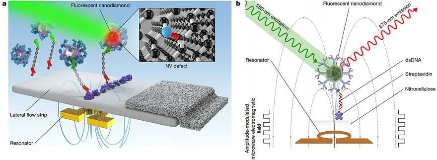
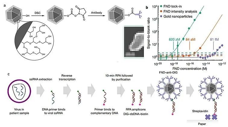
Spherical nanodiamonds not only have extremely high specific surface area, stability and biocompatibility, but also will not scratch the surface of application objects, such as biological skin, blood vessels and precision devices. They can be chemically modified to carry drugs. It has extremely high application value in the fields of beauty and skin care, drug transportation, targeted therapy, and electrochemical monitoring and sensing.
By designing the structure of the molybdenum tray, the researchers controlled the distribution of groups in the plasma to create a gas-phase nucleation space for nanodiamonds. The nanodiamond particles prepared by this method are purer than the detonation method and HPHT method. It breaks through the limitations of the output and film morphology of nanodiamonds prepared by the traditional CVD method. The particles not only have high yield, but also remain dispersed and have high crystallinity. They are widely used in medicines. It has strong application competitiveness in fields such as transportation, biological imaging, and quantum light sources.
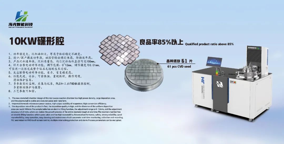
With MPCVD technology as its core, High Light Intelligence Technology has long been committed to the R&D and manufacturing of high-quality diamond materials and related equipment. It has advanced MPCVD equipment, laser processing equipment and precision polishing equipment. High Light Intelligence Technology's MPCVD technology equipment can produce high-quality diamond, thereby helping to improve the performance of integrated circuits. Our products and services are designed to provide customers with the best solutions to meet their needs for high quality diamond and integrated circuit performance.









-

CVD Single-Crystal Diamonds: An Analysis of the Complete Processing Workflow from Gas-Phase Deposition to Finished Diamond Chips
MPCVD (Microwave Plasma Chemical Vapor Deposition) technology is currently the core process for producing high-quality single-crystal diamond s. Thanks to its advantages of low defect rates, high purity, and controllable large dimensions, it is widely used in fields such as semiconductor heat dissipation, precision optics, and high-end sensors. The final quality of single-crystal diamond s depends on comprehensive process control throughout the entire workflow—from vapor deposition growth to pos
-
Single-Crystal or Polycrystalline Diamond — Which Has Greater Potential?
As diamond continues to enter industries such as semiconductors, thermal management, optics, high-power electronics, and precision machining, the requirements for diamond materials are also evolving.
-
Diamond Polishing and Grinding Processes: Core Challenges and Industry Hurdles
Diamond is often hailed as the “ultimate material” – ranking 10 on the Mohs hardness scale, boasting an ultra‑high thermal conductivity (~2,200 W/(m·K)), excellent chemical stability, and broad optical transparency. These properties make it irreplaceable in cutting‑edge applications such as semiconductor heat dissipation, high‑end optics, and quantum chips. Yet the paradox of “good materials are hard to process” is nowhere more evident than in diamond. From rough grinding for planarization to at
-
Single-Crystal vs Polycrystalline CVD Diamond: Process Difference Lies in Growth Logic, Not Equipment
The process difference between single crystal and polycrystalline CVD diamond lies not in equipment, but in growth logic. Single crystal and polycrystalline CVD diamond are two functional new materials with completely independent growth mechanisms, lattice structures and performance systems. Their process logic, product features and application boundaries diverge fundamentally from the very start of deposition and growth. Comparing or selecting materials without considering their underlying crys




