

- 中文
- English
- Español
What is the difference between semiconductor substrate and epitaxy?
2024-03-22 17:13:32
Click:
“
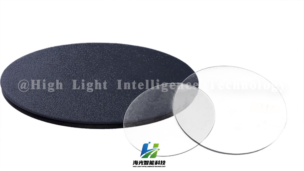
Silicon epitaxial layers and substrates are two important components in the semiconductor manufacturing process. The substrate is the basis for semiconductor chip manufacturing and is mainly made of single crystal silicon material. The silicon epitaxial layer is a layer of silicon material processed and grown on the substrate, and its material properties are the same as the substrate. Both are different in composition, structure and properties.
”
Silicon epitaxial layers and substrates are two important components in the semiconductor manufacturing process. The substrate is the basis for semiconductor chip manufacturing and is mainly made of single crystal silicon material. The silicon epitaxial layer is a layer of silicon material processed and grown on the substrate, and its material properties are the same as the substrate. Both are different in composition, structure and properties.
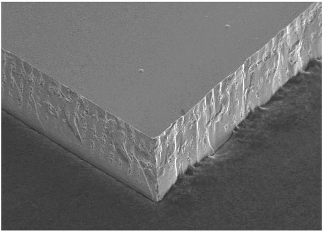

The value of epitaxial wafers is reflected in their ingenious combination of materials. For example, by growing a thin layer of GaN epitaxy on a lower-cost silicon wafer, it is possible to partially realize the wide bandgap characteristics of expensive and excellent third-generation semiconductors using relatively inexpensive first-generation semiconductor materials. , achieving high cost performance. However, heteroepitaxial structures are also accompanied by a series of challenges, such as lattice mismatch, inconsistent temperature coefficients and poor thermal conductivity. Just like building scaffolding on a plastic foundation, different materials will have differences in expansion and contraction when the temperature changes, and Silicon's thermal conductivity is not ideal.
Homoepitaxy, that is, growing an epitaxial layer that is the same as the substrate material on the substrate, is meant to further improve the stability and reliability of the product. Although the materials are the same, the material purity and uniformity on the wafer surface are significantly improved through epitaxy processing. Compared with mechanically polished polished wafers, the surface of epitaxial wafers is smoother and cleaner, with significantly reduced micro-defects and impurities, more uniform resistivity, and more precise control of defects such as surface particles, stacking faults, and dislocations. Therefore, epitaxy technology not only optimizes product performance, but also ensures product stability and reliability.
In the fields of modern electronics, optoelectronics, microelectronics and information technology, semiconductor substrates and epitaxial technologies play an indispensable role. They provide a solid foundation for manufacturing high-performance, high-reliability semiconductor devices. With the continuous development of science and technology, semiconductor substrate and epitaxial technology will also continue to advance, bringing new breakthroughs and developments to the future semiconductor industry.

![]()
With MPCVD technology as its core, High Light Intelligence Technology has long been committed to the R&D and manufacturing of high-quality diamond materials and related equipment. It has advanced MPCVD equipment, laser processing equipment and precision polishing equipment. High Light Intelligence Technology's MPCVD technology equipment can produce high-quality diamond, thereby helping to improve the performance of integrated circuits. Our products and services are designed to provide customers with the best solutions to meet their needs for high quality diamond and integrated circuit performance.


-

Z-Axis System: The Key to Stable Production of MPCVD Diamonds
Microwave Plasma Chemical Vapor Deposition is the mainstream method for producing high-quality diamonds in the industry. When the equipment is running, it first pumps the reaction chamber into a vacuum state to strictly ensure the chamber is fully sealed and airtight. Then, the microwave device releases energy, and special mixed reaction gases are fed into the chamber. Under the action of energy, a stable plasma area is formed. These highly active plasmas provide stable heat and reaction conditi
-
How to Choose the Right MPCVD Equipment?
MPCVD equipment is a critical asset across a wide range of industries, including industrial manufacturing, semiconductor thermal management, precision cutting tools, and lab-grown diamonds. Choosing the right equipment not only boosts production efficiency and ensures consistent product quality but also effectively controls long-term costs, making your entire production process smoother and more competitive. Many people struggle with the question: How do I make the right choice? Today, drawing o
-
CVD Diamond Clarity: How to Avoid Inclusions That Affect Jewelry Value
After selecting a loose diamond, the setting not only determines the diamond’s security but also directly affects its perceived size. With diamonds of the same weight, choosing the right setting design can effortlessly create the surprise of “small carats making a big impact,” saving on your budget while enhancing the diamond’s quality. Among these, pavé and prong settings are the two most classic and effective ways to make a diamond appear larger. Paired with specialized designs that maximize t
-
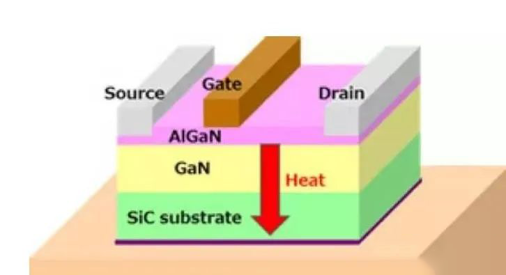
How Diamond Became the Ultimate Thermal Solution in the Era of Computing Power
The iconic narrative behind the legendary "A Diamond is Forever" slogan has long been upended by China's industrial prowess. Once synonymous with luxury and rarity, this gem has shed its glamorous aura to become an indispensable thermal management material for high-power devices. In an era of explosive growth in AI computing power, it has taken up the mantle of "cooling to save computing power".


