

- 中文
- English
- Español
Thermal Management at the GaN/Diamond Power Device Interface
2024-06-19 09:21:36
Click:
“
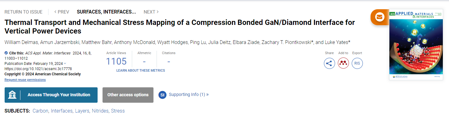
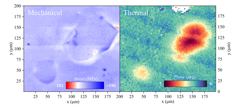
The demonstration of high breakdown voltage of gallium nitride (GaN) power devices has promoted the optimization of applications such as power electronics, as it can significantly improve conversion efficiency. GaN devices are available in two types: lateral and vertical. The lateral device electric field is arranged horizontally and confined to the GaN, while the vertical device electric field is evenly distributed, which can increase the breakdown voltage without increasing the chip size.
”
The demonstration of kilovolt breakdown voltages in gallium nitride (GaN) power devices has long inspired optimization in power electronics and other applications. This is due to the potential for greatly improved conversion efficiency in power systems. GaN devices can be divided into lateral and vertical device structures. In lateral devices, the electric field is aligned laterally in the device and is confined inside the GaN but close to the surface. In vertical devices, the electric field is evenly distributed within the GaN. Therefore, vertical devices can improve the breakdown voltage without increasing the chip size.
Text guide
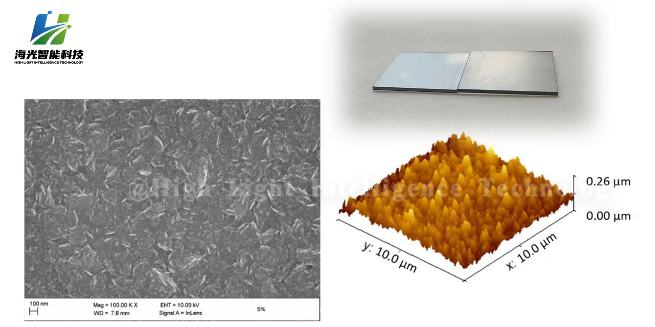

Image guide
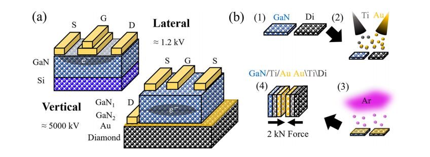
Figure 2. Schematic diagram of an electron microscope.


-

Z-Axis System: The Key to Stable Production of MPCVD Diamonds
Microwave Plasma Chemical Vapor Deposition is the mainstream method for producing high-quality diamonds in the industry. When the equipment is running, it first pumps the reaction chamber into a vacuum state to strictly ensure the chamber is fully sealed and airtight. Then, the microwave device releases energy, and special mixed reaction gases are fed into the chamber. Under the action of energy, a stable plasma area is formed. These highly active plasmas provide stable heat and reaction conditi
-
How to Choose the Right MPCVD Equipment?
MPCVD equipment is a critical asset across a wide range of industries, including industrial manufacturing, semiconductor thermal management, precision cutting tools, and lab-grown diamonds. Choosing the right equipment not only boosts production efficiency and ensures consistent product quality but also effectively controls long-term costs, making your entire production process smoother and more competitive. Many people struggle with the question: How do I make the right choice? Today, drawing o
-
CVD Diamond Clarity: How to Avoid Inclusions That Affect Jewelry Value
After selecting a loose diamond, the setting not only determines the diamond’s security but also directly affects its perceived size. With diamonds of the same weight, choosing the right setting design can effortlessly create the surprise of “small carats making a big impact,” saving on your budget while enhancing the diamond’s quality. Among these, pavé and prong settings are the two most classic and effective ways to make a diamond appear larger. Paired with specialized designs that maximize t
-
How Diamond Became the Ultimate Thermal Solution in the Era of Computing Power
The iconic narrative behind the legendary "A Diamond is Forever" slogan has long been upended by China's industrial prowess. Once synonymous with luxury and rarity, this gem has shed its glamorous aura to become an indispensable thermal management material for high-power devices. In an era of explosive growth in AI computing power, it has taken up the mantle of "cooling to save computing power".


