

- 中文
- English
- Español
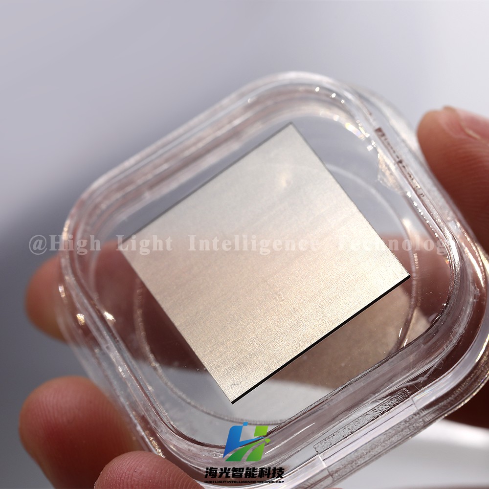
What are the advantages of CVD diamond chips?
2024-08-30 09:39:03
Click:
“
In an era where performance and efficiency are paramount, the technological innovation led by CVD diamond chips is emerging, illuminating the future of the semiconductor industry like a bright star. Let's explore the charm and unlimited potential of this technological pearl!
”
In the era of pursuing ultimate performance and efficiency, a technological revolution led by CVD diamond chips is quietly emerging. It is like a bright star, illuminating the future of the semiconductor industry. Today, let us explore the unique charm and infinite possibilities of this technological pearl together!
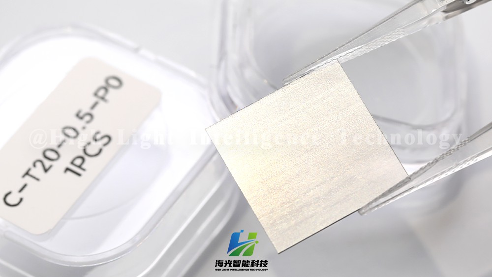
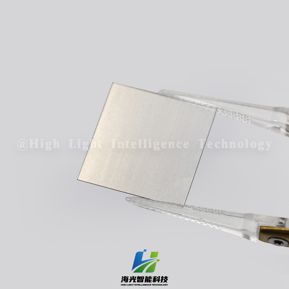
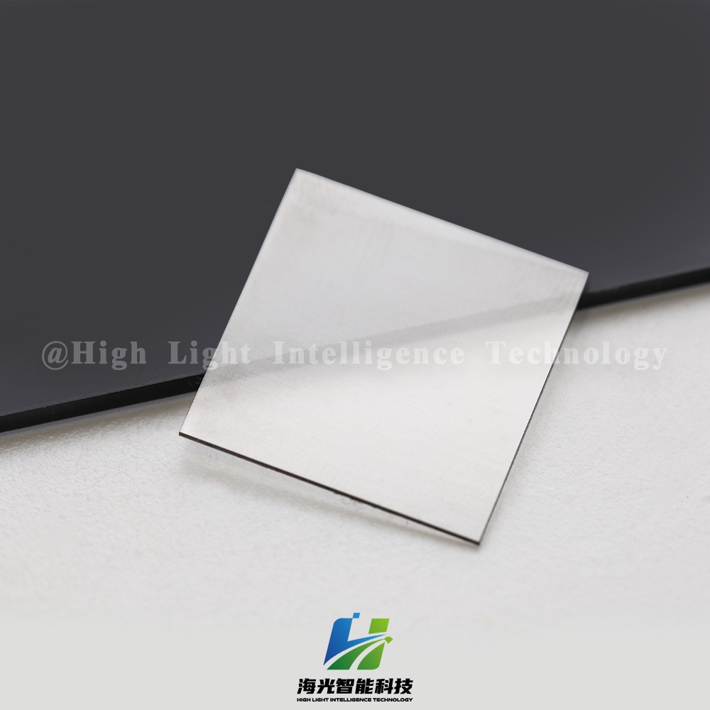

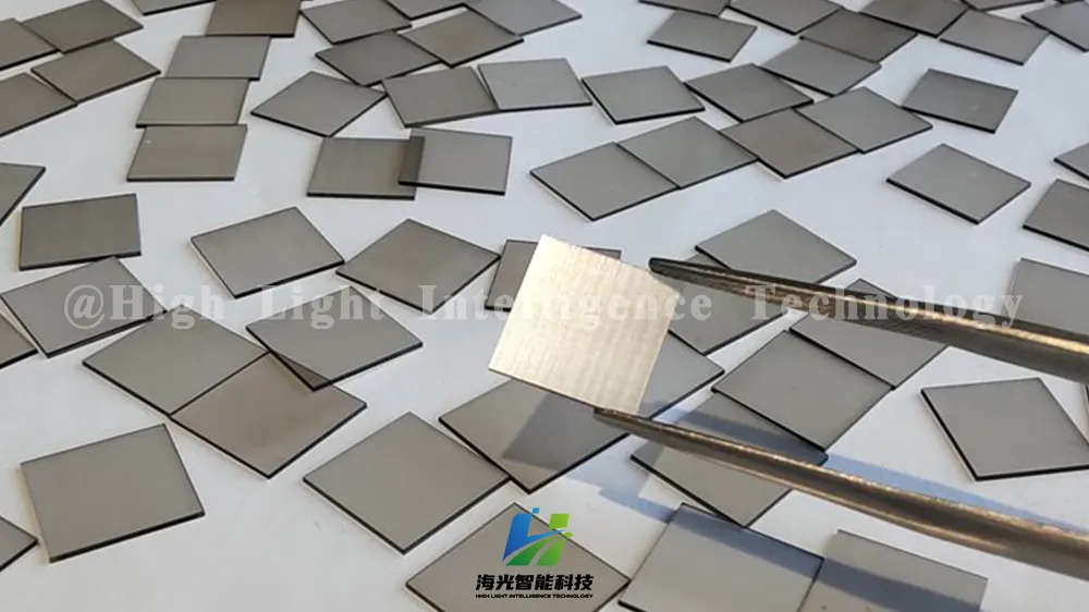
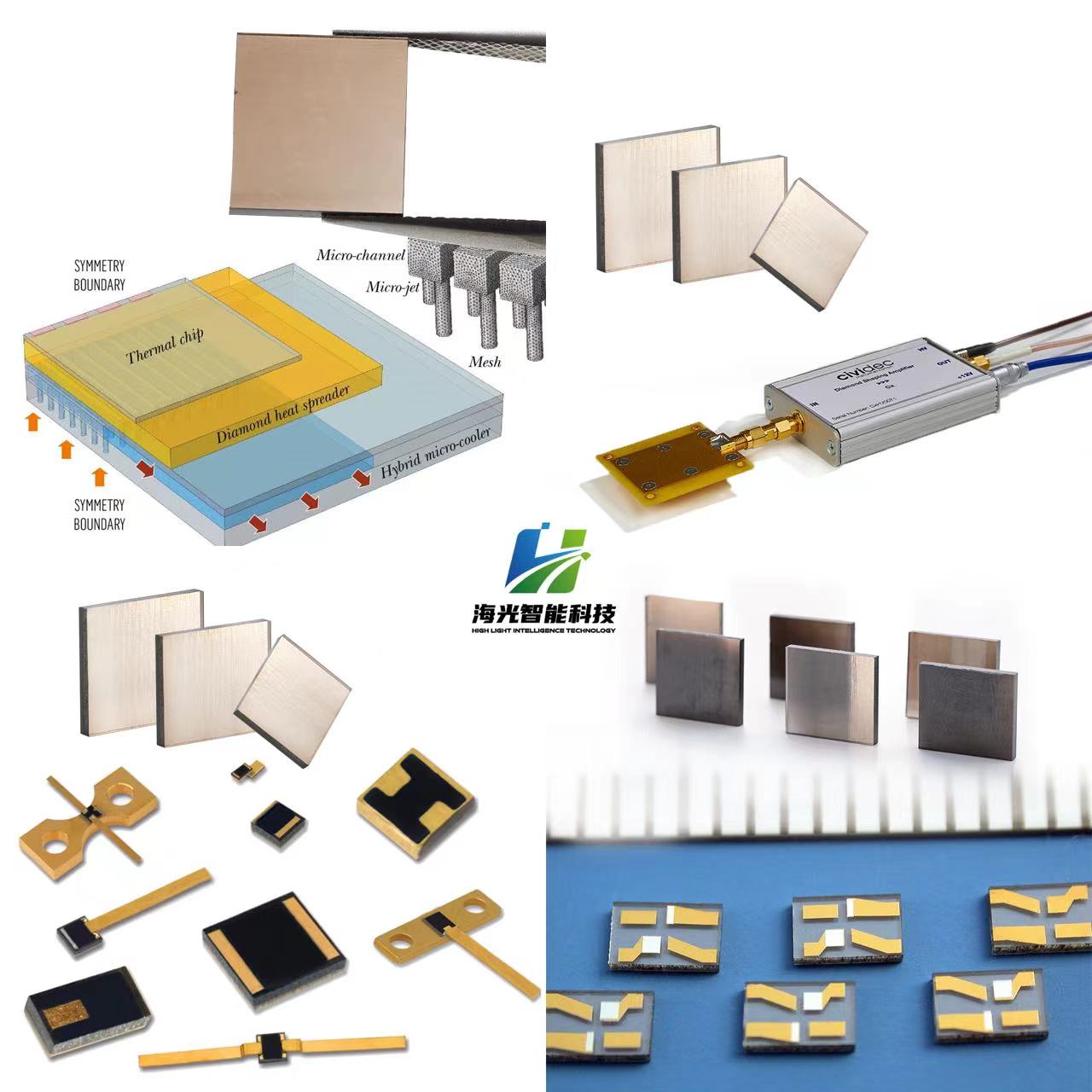
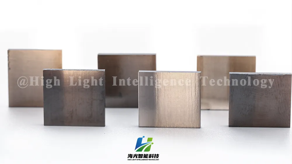
Diamond has become an efficient heat dissipation material with excellent heat dissipation performance, significantly reducing heat dissipation losses and ensuring stable high-temperature operation. When constructing converters, diamond devices reduce weight and capacity by half compared to silicon-based devices and one-third compared to silicon carbide devices. In the design, it is necessary to balance energy efficiency, cost, size, and weight, and diamond is particularly prominent in improving the energy efficiency of electric vehicles. In terms of cost, the design cost of diamond chips is about 30% lower than that of silicon carbide, due to less material demand and good thermal management. In terms of efficiency, diamond is reduced to one-third of silicon carbide, and its volume can be reduced by four times, resulting in significant energy savings. In terms of volume and weight optimization, diamond increases the switching frequency, reduces the volume of passive components by four times, simplifies the design of heat sinks, and promotes new breakthroughs in system lightweighting and compactness.
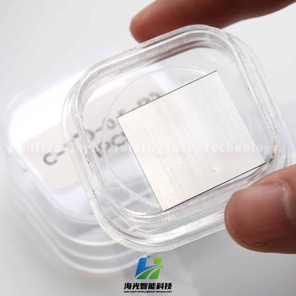
Diamond is known for its excellent insulation properties, with a breakdown electric field strength of up to 10 MV/cm, far exceeding silicon, SiC, and GaN. Even in thin sheet form, it maintains high insulation and high voltage resistance. In the field of 5G, diamond substrates, with their excellent thermal conductivity, help dissipate heat from high-power components, ensure stable operation, and meet the urgent need for efficient heat dissipation in 5G equipment. With the surge of 5G data, diamond substrates have become the key to solving the challenges of high frequency and high power density.
Compared with silicon-based technology, the combination of diamond with gallium nitride and silicon carbide can create high-performance power devices, which are widely used in fields such as electric vehicles, renewable energy, industrial drives, and high-power lasers, improving energy efficiency and extending equipment life. As an efficient radiator, it promotes the transition to clean energy and vehicle electrification, reduces energy loss, and improves system efficiency, especially suitable for space constrained scenarios such as electric vehicles.
Market forecasts show that the global diamond semiconductor substrate market is growing rapidly, expected to reach 342 million US dollars by 2030, with a CAGR of 12.3%. The Asia Pacific region, especially China, Japan, and South Korea, will dominate the market due to strong demand for electronic semiconductors, contributing over 40% of global revenue.


-

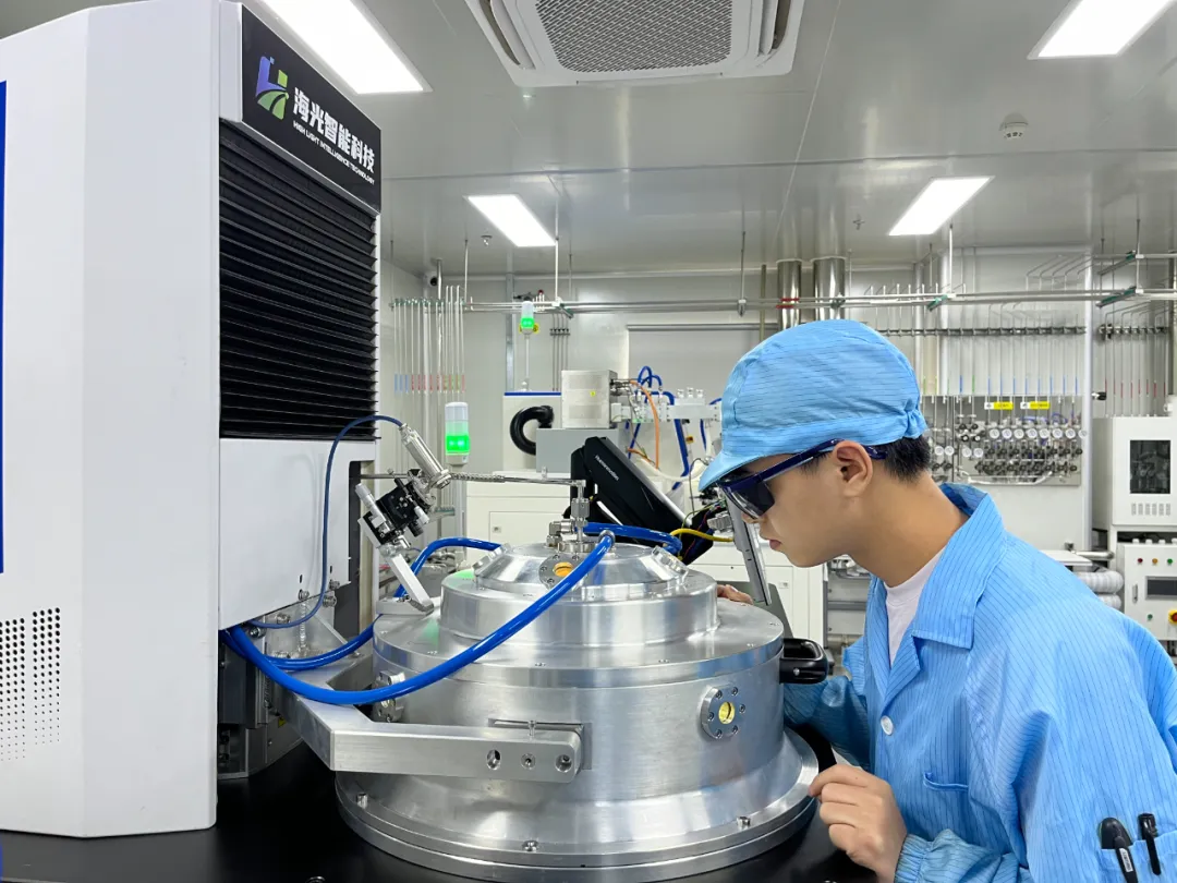
Z-Axis System: The Key to Stable Production of MPCVD Diamonds
Microwave Plasma Chemical Vapor Deposition is the mainstream method for producing high-quality diamonds in the industry. When the equipment is running, it first pumps the reaction chamber into a vacuum state to strictly ensure the chamber is fully sealed and airtight. Then, the microwave device releases energy, and special mixed reaction gases are fed into the chamber. Under the action of energy, a stable plasma area is formed. These highly active plasmas provide stable heat and reaction conditi
-
How to Choose the Right MPCVD Equipment?
MPCVD equipment is a critical asset across a wide range of industries, including industrial manufacturing, semiconductor thermal management, precision cutting tools, and lab-grown diamonds. Choosing the right equipment not only boosts production efficiency and ensures consistent product quality but also effectively controls long-term costs, making your entire production process smoother and more competitive. Many people struggle with the question: How do I make the right choice? Today, drawing o
-
CVD Diamond Clarity: How to Avoid Inclusions That Affect Jewelry Value
After selecting a loose diamond, the setting not only determines the diamond’s security but also directly affects its perceived size. With diamonds of the same weight, choosing the right setting design can effortlessly create the surprise of “small carats making a big impact,” saving on your budget while enhancing the diamond’s quality. Among these, pavé and prong settings are the two most classic and effective ways to make a diamond appear larger. Paired with specialized designs that maximize t
-
How Diamond Became the Ultimate Thermal Solution in the Era of Computing Power
The iconic narrative behind the legendary "A Diamond is Forever" slogan has long been upended by China's industrial prowess. Once synonymous with luxury and rarity, this gem has shed its glamorous aura to become an indispensable thermal management material for high-power devices. In an era of explosive growth in AI computing power, it has taken up the mantle of "cooling to save computing power".


