- 中文
- English
- Español
Nanodiamond, a major breakthrough!
2025-01-10 10:04:43
Click:
“
In recent decades, the combination of quantum technology and nanomaterials has brought about great changes in science and technology, especially the emergence of fluorescent nanodiamonds (FNDs), which have shown great potential in quantum sensing and biomedicine. FNDs play an important role in biological detection, quantum computing and extreme environment sensing due to their excellent physical stability and optical properties.
”
Key properties of fluorescent nanodiamonds
The leap from micrometers to nanometers
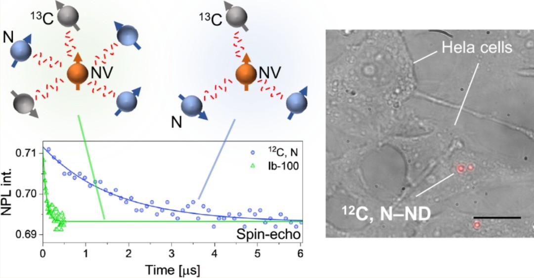
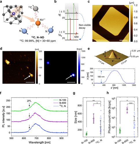
Improving the brightness and quantum performance of fluorescent nanodiamonds is an application obstacle. Researchers at the University of Florida used high pressure and high temperature methods and electron beam irradiation technology to synthesize 50-700 nanometer high-purity nanodiamonds with a nitrogen-vacancy concentration of 0.6-1.3ppm and 99.99% 12C to reduce impurity interference. After the improvement, the brightness was significantly improved, the contrast of the magnetic resonance signal only required 1/20 of the traditional microwave power, and the spin relaxation time was extended by 5-11 times, approaching the performance of bulk diamonds, laying the foundation for high-sensitivity biological detection.
Applications in biomedicine
Fluorescent nanodiamonds are used in biomedicine for high-resolution imaging and biosensing. They can be functionalized as biomarker molecules to track cell structures, and use NV centers to monitor changes in the cell microenvironment, such as achieving real-time intracellular temperature measurement (quantum thermal measurement), with sensitivity far exceeding that of traditional sensors. At the same time, they have great potential in drug delivery, can accurately deliver and track drug release, and provide new possibilities for personalized medicine.

Extreme environment sensing and quantum technology
Fluorescent nanodiamonds have outstanding performance in extreme environment sensing, and can withstand high temperature, high pressure and strong radiation, while maintaining quantum performance. In geological exploration, they can measure changes in the earth's crust magnetic field and help predict earthquakes and other activities. They also have great potential in the field of quantum computing. The NV center quantum spin can store operational information and is expected to become the core of quantum computers. Its quantum bits are superior to others in coherence time and anti-interference, which is of great significance to quantum computing and communications.
Challenges and prospects
Fluorescent nanodiamonds have broad prospects, but they face technical and application challenges, such as high cost, insufficient preparation consistency, and safety and functionalization issues in biomedical applications. With the advancement of quantum material technology, these problems are expected to be solved. In the future, fluorescent nanodiamonds may be used in high-performance batteries, environmental monitoring, optoelectronic devices, etc., and may enter the consumer field due to cost reduction, such as high-end cosmetics and smart wearable devices.
Conclusion
Fluorescent nanodiamond combines quantum and nanotechnology, and leads scientific research and application innovation with its unique optical and quantum properties, covering biomedicine, quantum computing, environmental sensing and personalized medicine. In the future, it will continue to promote the frontier of science and technology and help humans explore the unknown.

High Light Intelligence Technology, a pioneer in the CVD diamond industry, has advanced MPCVD technology and CVD diamond production workshops. We focus on producing high-purity lab-grown diamonds for the jewelry industry, and at the same time create industrial-grade CVD diamond products, covering single crystals, polycrystalline, films and diamond surface metallization. We also provide 6kw/10kw/15kw MPCVD equipment to help customers in all aspects, from equipment to products, and then to all-round services, to create brilliance together.
*The articles and pictures are only for industry communication and sharing. If there is any infringement, please contact us to delete them.









-

Single-Crystal vs Polycrystalline CVD Diamond: Process Difference Lies in Growth Logic, Not Equipment
The process difference between single crystal and polycrystalline CVD diamond lies not in equipment, but in growth logic. Single crystal and polycrystalline CVD diamond are two functional new materials with completely independent growth mechanisms, lattice structures and performance systems. Their process logic, product features and application boundaries diverge fundamentally from the very start of deposition and growth. Comparing or selecting materials without considering their underlying crys
-
From Lab-Grown Diamonds to Industrial Diamonds: Is It Time to Build an MPCVD Factory?
The lab-grown diamond industry is entering a new stage. Over the these few years, lab-grown diamonds have gradually gained wider acceptance in the jewelry market. With the development of production technology, equipment maturity and supply chain improvement, the industry is becoming more standardized and efficient. But beyond jewelry, another opportunity is attracting more attention:Industrial diamond applications.
-
Diamond‑Copper Composite: A Next‑Generation Solution for High‑Power Electronics Thermal Management
Diamond‑copper composite (DC) is an advanced metal‑matrix composite material consisting of diamond particles as the reinforcement phase and copper as the matrix, fabricated through state‑of‑the‑art composite preparation techniques. Diamond has the highest thermal conductivity of any naturally occurring material, with isotropic values ranging from 1200 to 2300 W/m·K. Copper, with a thermal conductivity of 401 W/m·K, ranks second only to silver among common metals. By combining the two, the compo
-
Mosaic Single‑Crystal Diamond: Breaking Size Limits
With an ultra‑wide bandgap of 5.47 eV, ultra‑high thermal conductivity (>2000 W/m·K), high carrier mobility (electron mobility up to 4500 cm²·V⁻¹·s⁻¹), and ultra‑high theoretical breakdown field strength (>10 MV/cm), Single‑Crystal Diamond (SCD) is an ideal candidate for next‑generation high‑power, high‑frequency and extreme‑environment electronic devices. However, both natural diamond and HPHT‑synthesized single‑crystal diamond are limited in lateral size, which greatly hinders large‑scal