

- 中文
- English
- Español
How diamond, the king of heat dissipation, helps the electronics industry take off
2024-01-31 13:37:36
Click:
“
The popularity of lab-grown diamonds lies not only in the jewelry industry, but also in high-precision industrial fields. As the king of materials, diamond has many excellent physical and chemical properties. Diamond single crystal is the ultimate semiconductor material. It combines excellent crystallinity, extremely high breakdown voltage, excellent electrical properties and extremely high thermal conductivity. The most outstanding thing is its high thermal conductivity. At 30-650°C, diamond is
”
The popularity of lab-grown diamonds lies not only in the jewelry industry, but also in high-precision industrial fields. As the king of materials, diamond has many excellent physical and chemical properties. Diamond single crystal is the ultimate semiconductor material. It combines excellent crystallinity, extremely high breakdown voltage, excellent electrical properties and extremely high thermal conductivity. The most outstanding thing is its high thermal conductivity. At 30-650°C, diamond is the crystal with the highest thermal conductivity among solid materials.
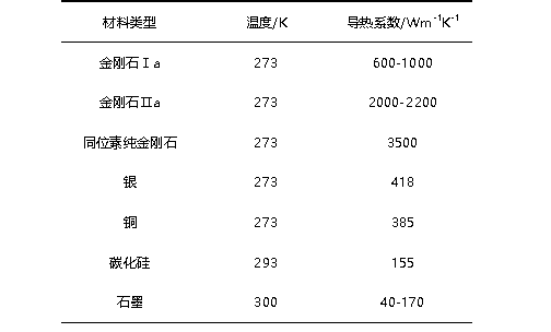
The thermal conductivity of a crystal is determined by the heat capacity, phonon mean free path, and phonon speed. The anharmonic vibration of the diamond lattice is weak and the phonon mean free path is long; the Debye temperature is high and the phonon speed is fast, so the thermal conductivity The rate is extremely high. At room temperature, the thermal conductivity of diamond is five times that of copper and 15 times that of silicon, which has obvious advantages over other materials.
Single crystal diamond has the highest thermal conductivity among diamond materials, which is closely related to its crystal structure. It mainly conducts heat through lattice vibration, that is, phonons. There are two main ways to use single crystal diamond for heat dissipation. One is to directly use it as a replacement epitaxial substrate, grow the material in situ to prepare the device, and make close contact with the diamond through the active area of the device, using the ultra-high thermal conductivity of diamond to evenly distribute heat into the substrate. The other is to add a microchannel structure to the single crystal diamond structure and use fluid to take out the internal heat to achieve the purpose of cooling.
Large-area single crystal diamond substrates mainly provide epitaxial growth substrates for the development and industrialization of various electronic devices. High-power diamond power electronic devices: It can replace existing Si, SiC and other power conversion devices and switching power supplies, greatly reduce the size of the conversion device, and does not require heat dissipation, achieving a significant increase in conversion efficiency and a significant reduction in power consumption, improving reliability Significant improvement. The energy consumption of diamond electronic devices will be 1/3-1/5 of the devices currently used.
Ultra-high frequency and high-power diamond electronic devices (microwave, millimeter wave radar): can be used in fire control weapon systems, radar, high-speed wireless communications, rockets, aerospace and other fields. It can replace the currently used traveling wave tubes, making weapon systems and communication systems more miniaturized and greatly improved in reliability, greatly increasing the data transmission rate of communication systems, and significantly reducing the weight, launch costs and radiation resistance of satellites and other spacecrafts. ability.
Applied to integrated circuit chips: Develop next-generation diamond-based integrated circuit chips to completely solve the heat dissipation bottleneck problem of integrated circuits and make integrated circuits larger-scale and faster. Diamond UV LED, LD: can be used in environmental protection and medical sterilization, high-density data storage, etc. Biosensors such as DNA: Use the affinity of diamond to biological cells and the high sensitivity of biosensors to develop various diamond biosensors; at the same time, they can also be made into biological weapons detectors. Sun-blind ultraviolet detectors and ultrafast particle radiation scintillator detectors: used in missile guidance and early warning, and deep space X-ray communications.
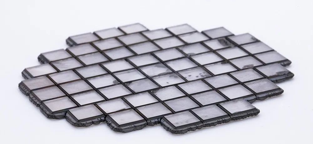
At present, various technical forms have been developed to use diamond as a heat sink or substrate for power devices, among which the main ones are: diamond bonding based on substrate transfer technology, low-temperature deposition based on diamond passivation layer, and device epitaxial growth on diamond. . At this stage, room temperature bonding of polycrystalline diamond with Si, GaN, Ga2O3, etc. has been achieved through surface activation bonding (SAB) technology.
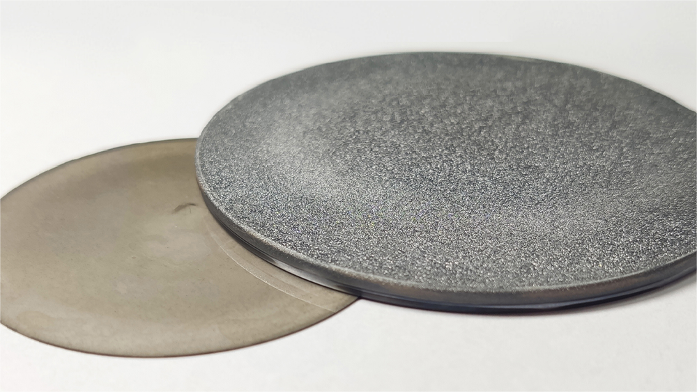
Polycrystalline diamond has high performance advantages as a heat sink for high-power chips and electronic devices. In the future, as production increases and costs decrease, it is expected to be widely used in the field of semiconductor heat sinks. At present, commercial mass production of 4-inch electronic-grade polycrystalline diamond has been achieved, and the international maximum preparation size can reach 8 inches. With the improvement and upgrading of MPCVD technology, it is expected to be compatible with the existing 8-inch semiconductor wafer manufacturing line, and finally achieve multi-crystalline diamond production. The large-scale application and promotion of diamond heat sink materials in the semiconductor material industry.
Nano diamond materials are generally used for heat dissipation as a passivation layer for devices with high heat flux density. They can evenly heat the surface of the device, add a heat conduction path to the device, and improve the temperature uniformity performance of the device surface. Hydrogen plasma has a reactive etching effect on gallium nitride, causing the method of directly depositing diamond on the device to require low temperature conditions and a hydrogen-resistant design. On the surface of the hydrogen-resistant protective layer, diamond needs to be nucleated uniformly and at a high density, and at the same time, it needs to be highly oriented to improve the overall thermal conductivity of the diamond passivation layer.
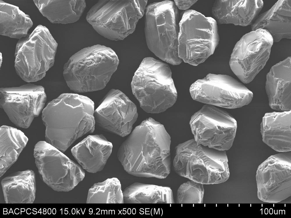
Harbin Institute of Technology cooperated with China Electronics Technology Group Co., Ltd. 55 to develop nano-diamond passivated GaN devices. The nano-diamond passivation layer with controllable grain size was prepared at 600°C to achieve full coverage of the device surface with a highly thermally conductive diamond layer. However, There is still a problem that the thermal conductivity of nanodiamond is worse than that of single crystal and the heat dissipation effect is limited. There is still room for further exploration.
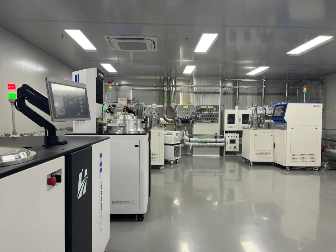
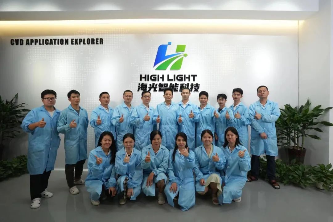
Whether it is single crystal or polycrystalline products, High Light Intelligence Technology shows excellent performance and quality. Customers can choose products that suit them according to their own needs. Haiguang Intelligent Technology is a semiconductor diamond production supplier. While the semiconductor industry is developing rapidly, we also provide diamond materials to major commercial customers and academic researchers, contributing to the development of semiconductor technology and materials. With MPCVD technology as the core, we have long been committed to the R&D and manufacturing of high-quality diamond materials and related equipment. We have advanced MPCVD equipment, laser processing equipment and precision polishing equipment.
作者:佛山市海光智能科技有限公司


-

Z-Axis System: The Key to Stable Production of MPCVD Diamonds
Microwave Plasma Chemical Vapor Deposition is the mainstream method for producing high-quality diamonds in the industry. When the equipment is running, it first pumps the reaction chamber into a vacuum state to strictly ensure the chamber is fully sealed and airtight. Then, the microwave device releases energy, and special mixed reaction gases are fed into the chamber. Under the action of energy, a stable plasma area is formed. These highly active plasmas provide stable heat and reaction conditi
-
How to Choose the Right MPCVD Equipment?
MPCVD equipment is a critical asset across a wide range of industries, including industrial manufacturing, semiconductor thermal management, precision cutting tools, and lab-grown diamonds. Choosing the right equipment not only boosts production efficiency and ensures consistent product quality but also effectively controls long-term costs, making your entire production process smoother and more competitive. Many people struggle with the question: How do I make the right choice? Today, drawing o
-
CVD Diamond Clarity: How to Avoid Inclusions That Affect Jewelry Value
After selecting a loose diamond, the setting not only determines the diamond’s security but also directly affects its perceived size. With diamonds of the same weight, choosing the right setting design can effortlessly create the surprise of “small carats making a big impact,” saving on your budget while enhancing the diamond’s quality. Among these, pavé and prong settings are the two most classic and effective ways to make a diamond appear larger. Paired with specialized designs that maximize t
-
How Diamond Became the Ultimate Thermal Solution in the Era of Computing Power
The iconic narrative behind the legendary "A Diamond is Forever" slogan has long been upended by China's industrial prowess. Once synonymous with luxury and rarity, this gem has shed its glamorous aura to become an indispensable thermal management material for high-power devices. In an era of explosive growth in AI computing power, it has taken up the mantle of "cooling to save computing power".


