- 中文
- English
- Español
High Light Intelligence Technology shines at the 6th Shenzhen International Semiconductor Exhibition!
2024-06-28 16:12:58
Click:
“
On the second day of the exhibition, High Light Intelligence Technology once again shined on the stage of the 6th Shenzhen International Semiconductor Exhibition! As a leader in the field of CVD diamond, we brought a number of cutting-edge products to the exhibition, and joined the global industry colleagues to explore a new chapter in semiconductor technology.
”
On the second day of the exhibition, High Light Intelligence Technology once again shined on the stage of the 6th Shenzhen International Semiconductor Exhibition! As a leader in the field of CVD diamond, we brought a number of cutting-edge products to the exhibition, and joined the global industry colleagues to explore a new chapter in semiconductor technology.

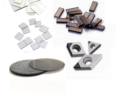
At the exhibition, High Light Intelligence Technology's CVD diamond products became the focus of attention, and its hardness, thermal stability, chemical stability, and excellent electrical and optical properties were highly praised. With professional skills, the business team demonstrated the core position of diamond in semiconductor device manufacturing. At the same time, we also demonstrated the latest CVD diamond preparation technology and R&D progress, which not only improved product performance, but also provided customers with more efficient and high-quality services.
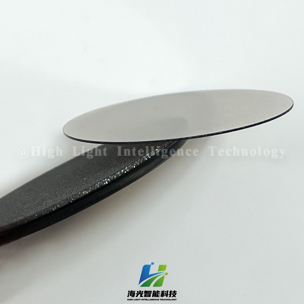
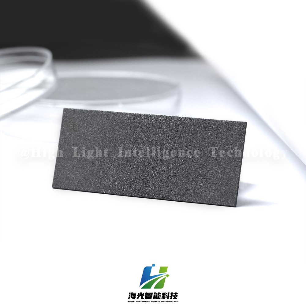
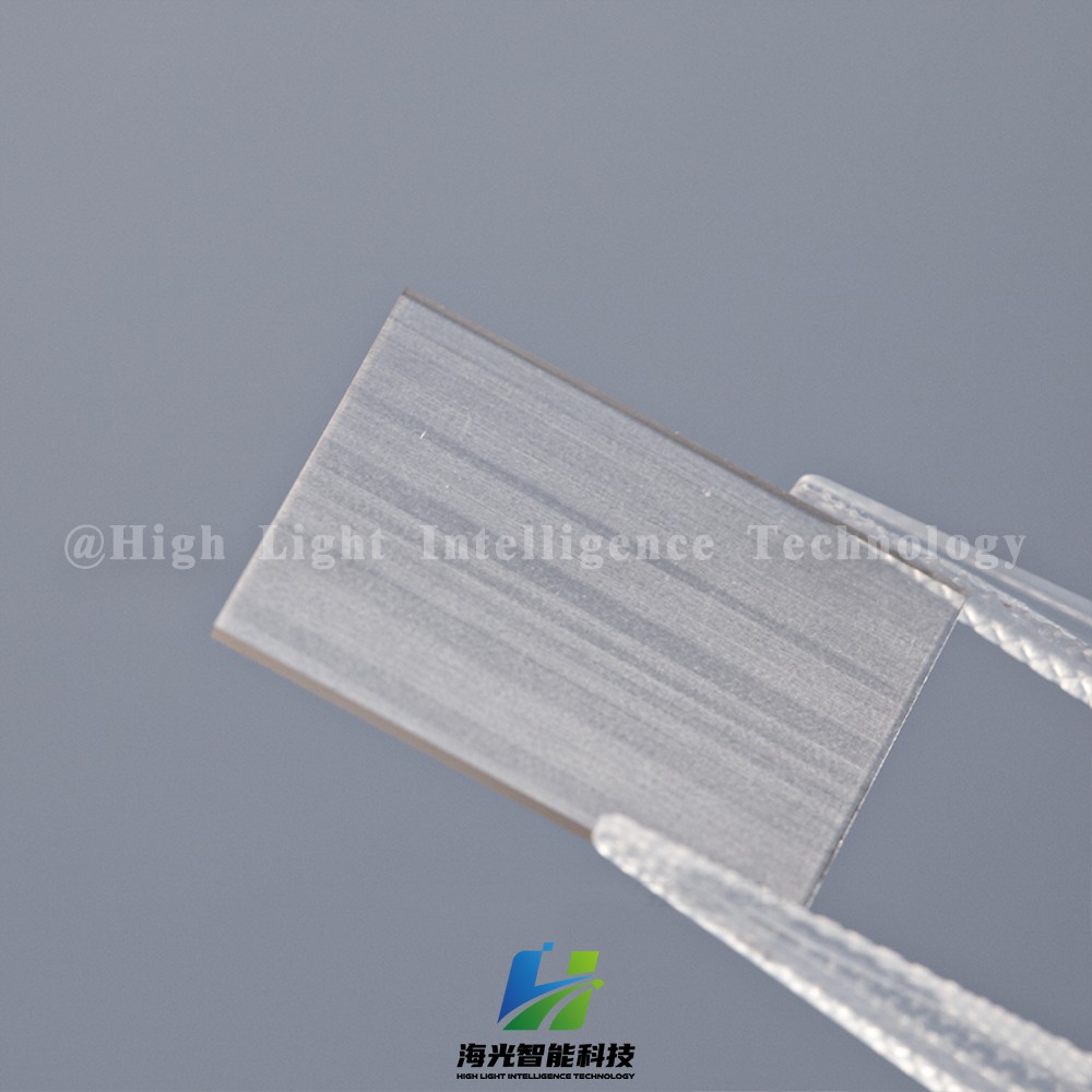
The semiconductor industry is highly competitive, and exhibitors are showcasing innovative technologies. High Light Intelligence Technology has successfully applied its leading CVD diamond preparation process and technical advantages to photonic devices, driving industry progress. At the exhibition, we showcased the latest CVD diamond preparation technology and R&D progress, improving product performance and quality, and providing customers with more efficient and high-quality services. We firmly believe that innovation is the key to competition, and we will continue to improve product quality to remain invincible.

In-depth Exchanges and Common Development











-

Single-Crystal vs Polycrystalline CVD Diamond: Process Difference Lies in Growth Logic, Not Equipment
The process difference between single crystal and polycrystalline CVD diamond lies not in equipment, but in growth logic. Single crystal and polycrystalline CVD diamond are two functional new materials with completely independent growth mechanisms, lattice structures and performance systems. Their process logic, product features and application boundaries diverge fundamentally from the very start of deposition and growth. Comparing or selecting materials without considering their underlying crys
-
From Lab-Grown Diamonds to Industrial Diamonds: Is It Time to Build an MPCVD Factory?
The lab-grown diamond industry is entering a new stage. Over the these few years, lab-grown diamonds have gradually gained wider acceptance in the jewelry market. With the development of production technology, equipment maturity and supply chain improvement, the industry is becoming more standardized and efficient. But beyond jewelry, another opportunity is attracting more attention:Industrial diamond applications.
-
Diamond‑Copper Composite: A Next‑Generation Solution for High‑Power Electronics Thermal Management
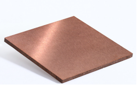
Diamond‑copper composite (DC) is an advanced metal‑matrix composite material consisting of diamond particles as the reinforcement phase and copper as the matrix, fabricated through state‑of‑the‑art composite preparation techniques. Diamond has the highest thermal conductivity of any naturally occurring material, with isotropic values ranging from 1200 to 2300 W/m·K. Copper, with a thermal conductivity of 401 W/m·K, ranks second only to silver among common metals. By combining the two, the compo
-
Mosaic Single‑Crystal Diamond: Breaking Size Limits
With an ultra‑wide bandgap of 5.47 eV, ultra‑high thermal conductivity (>2000 W/m·K), high carrier mobility (electron mobility up to 4500 cm²·V⁻¹·s⁻¹), and ultra‑high theoretical breakdown field strength (>10 MV/cm), Single‑Crystal Diamond (SCD) is an ideal candidate for next‑generation high‑power, high‑frequency and extreme‑environment electronic devices. However, both natural diamond and HPHT‑synthesized single‑crystal diamond are limited in lateral size, which greatly hinders large‑scal