

- 中文
- English
- Español
CVD Single-Crystal Diamonds: An Analysis of the Complete Processing Workflow from Gas-Phase Deposition to Finished Diamond Chips
2026-09-18 15:39:55
Click:
“
MPCVD (Microwave Plasma Chemical Vapor Deposition) technology is currently the core process for producing high-quality single-crystal diamond s. Thanks to its advantages of low defect rates, high purity, and controllable large dimensions, it is widely used in fields such as semiconductor heat dissipation, precision optics, and high-end sensors. The final quality of single-crystal diamond s depends on comprehensive process control throughout the entire workflow—from vapor deposition growth to pos
”
MPCVD (Microwave Plasma Chemical Vapor Deposition) technology is currently the core process for producing high-quality single-crystal diamond s. Thanks to its advantages of low defect rates, high purity, and controllable large dimensions, it is widely used in fields such as semiconductor heat dissipation, precision optics, and high-end sensors. The final quality of single-crystal diamond s depends on comprehensive process control throughout the entire workflow—from vapor deposition growth to post-processing precision machining. The precision control in each process step directly determines the ’s flatness, light transmittance, thermal conductivity, and service life. This article provides a comprehensive breakdown of the entire manufacturing chain for MPCVD single-crystal diamond s, from raw material deposition to final product delivery.

Seed crystal pretreatment and chemical vapor deposition (CVD) growth are the foundational steps in fabrication. After pretreatment, the seed crystal is placed in the MPCVD vacuum chamber. By precisely controlling microwave power, chamber temperature and pressure, and the hydrocarbon gas ratio, active carbon atoms are induced to grow epitaxially along the seed crystal’s lattice. After a period of stable deposition, a pure CVD single-crystal diamond rough with a dense texture, uniform crystal lattice, and low defect rate is produced.
After the roughing process is complete, high-precision laser shaping and cutting are required—a core process for controlling the ’s basic dimensions and base surface accuracy. The edges of MPCVD-grown diamond roughing typically exhibit polycrystalline mixed layers, growth stress zones, and irregular contours. During production, residual seed crystals and the transition growth layer are first removed, followed by shaping and dimensional cutting using high-precision laser cutting equipment. Compared to traditional mechanical cutting processes, laser cutting involves no mechanical contact and generates minimal stress, effectively preventing defects such as chipping, cracking, and deformation, and accommodating the processing needs of customized s in various specifications. After laser cutting, the base surfaces of our single-crystal s are uniform and regular, with surface roughness consistently controlled below 600 nm, laying a solid foundation for subsequent ultra-precision polishing.

Precision grinding and graded ultra-precision polishing are critical processing steps that determine the ’s final quality, optical performance, and thermal conductivity. To address residual marks and microscopic flatness issues on the ’s base surface after cutting, we employ a graded precision machining process to progressively correct surface accuracy and eliminate residual surface stress. After conventional general polishing, the surface roughness can be optimized to 5–10 nm, thoroughly removing fine cutting marks and surface irregularities left by the cutting process to achieve a uniform and flat base surface. For high-precision applications such as high-power semiconductors, precision optics, and high-end detection devices, nano-level ultra-precision polishing can be performed to control the surface roughness to<1 nm. Throughout the entire polishing process, core parameters such as total thickness variation (TTV), flatness, and parallelism are strictly controlled to maximize the material advantages of single-crystal diamond—including high thermal conductivity, high light transmittance, and high stability—thereby meeting the stringent performance standards of high-end precision devices.

After polishing, the single-crystal s undergo dust-free cleaning and comprehensive quality inspection. The products undergo multiple specialized cleaning processes in a cleanroom to remove polishing powder, fine dust, and various trace residues from the surface. Subsequently, precision testing equipment is used to verify key indicators such as flatness, surface finish, and lattice integrity item by item, rigorously selecting only qualified products to ensure that shipped products maintain stable precision and meet performance standards.
Leveraging our mature, in-house developed processing technology, our company is capable of consistently mass-producing CVD single-crystal diamond s with nanoscale surface roughness. The combination of high-quality, pure CVD single-crystal substrates and refined post-processing techniques endows the finished s with extremely high structural density and lattice integrity. With a thermal conductivity of up to 2000 W/(m·K), these s exhibit outstanding physical properties, including highly efficient heat dissipation and high-temperature resistance. If you have any requirements, please feel free to contact our professional team for customization.
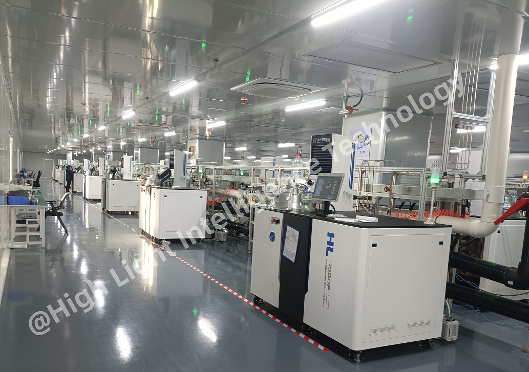
High Light Intelligence Technology, a pioneer in the CVD diamond industry, has advanced MPCVD technology and CVD diamond production workshops. We focus on producing high-purity lab-grown diamonds for the jewelry industry, and at the same time create industrial-grade CVD diamond products, covering single crystals, polycrystalline, films and diamond surface metallization. We also provide 6kw/10kw/15kw MPCVD equipment to help customers in all aspects, from equipment to products, and then to all-round services, to create brilliance together.









-

CVD Single-Crystal Diamonds: An Analysis of the Complete Processing Workflow from Gas-Phase Deposition to Finished Diamond Chips
MPCVD (Microwave Plasma Chemical Vapor Deposition) technology is currently the core process for producing high-quality single-crystal diamond s. Thanks to its advantages of low defect rates, high purity, and controllable large dimensions, it is widely used in fields such as semiconductor heat dissipation, precision optics, and high-end sensors. The final quality of single-crystal diamond s depends on comprehensive process control throughout the entire workflow—from vapor deposition growth to pos
-
Single-Crystal or Polycrystalline Diamond — Which Has Greater Potential?
As diamond continues to enter industries such as semiconductors, thermal management, optics, high-power electronics, and precision machining, the requirements for diamond materials are also evolving.
-
Diamond Polishing and Grinding Processes: Core Challenges and Industry Hurdles
Diamond is often hailed as the “ultimate material” – ranking 10 on the Mohs hardness scale, boasting an ultra‑high thermal conductivity (~2,200 W/(m·K)), excellent chemical stability, and broad optical transparency. These properties make it irreplaceable in cutting‑edge applications such as semiconductor heat dissipation, high‑end optics, and quantum chips. Yet the paradox of “good materials are hard to process” is nowhere more evident than in diamond. From rough grinding for planarization to at
-
Single-Crystal vs Polycrystalline CVD Diamond: Process Difference Lies in Growth Logic, Not Equipment
The process difference between single crystal and polycrystalline CVD diamond lies not in equipment, but in growth logic. Single crystal and polycrystalline CVD diamond are two functional new materials with completely independent growth mechanisms, lattice structures and performance systems. Their process logic, product features and application boundaries diverge fundamentally from the very start of deposition and growth. Comparing or selecting materials without considering their underlying crys



