

- 中文
- English
- Español
Diamond Polishing and Grinding Processes: Core Challenges and Industry Hurdles
2026-09-18 14:29:20
Click:
“
Diamond is often hailed as the “ultimate material” – ranking 10 on the Mohs hardness scale, boasting an ultra‑high thermal conductivity (~2,200 W/(m·K)), excellent chemical stability, and broad optical transparency. These properties make it irreplaceable in cutting‑edge applications such as semiconductor heat dissipation, high‑end optics, and quantum chips. Yet the paradox of “good materials are hard to process” is nowhere more evident than in diamond. From rough grinding for planarization to at
”
Diamond is often hailed as the “ultimate material” – ranking 10 on the Mohs hardness scale, boasting an ultra‑high thermal conductivity (~2,200 W/(m·K)), excellent chemical stability, and broad optical transparency. These properties make it irreplaceable in cutting‑edge applications such as semiconductor heat dissipation, high‑end optics, and quantum chips. Yet the paradox of “good materials are hard to process” is nowhere more evident than in diamond. From rough grinding for planarization to atomic‑level finishing, every step in the polishing and grinding workflow demands a delicate balance between precision, efficiency, and damage control.
1. Intrinsic Material Barriers
The difficulty of machining diamond stems from three fundamental characteristics:
1.1 Extreme Hardness – Tooling Struggles to Keep Up
Diamond is the hardest known natural material. Conventional abrasives are ineffective; machining relies almost exclusively on super‑hard grits (diamond particles) or energy‑beam techniques. This leads to rapid tool wear and escalating costs. Even when using diamond‑grit‑loaded polishing plates, high rotational speeds and heavy loads are required – not only causing uneven plate wear but also generating frictional heat that can induce a phase transformation from sp³ (diamond) to sp² (graphite) on the surface, softening the material and degrading surface quality.
1.2 Anisotropy – Different Crystal Faces, Different Hardness
Single‑crystal diamond exhibits significant hardness variations across different crystallographic orientations. Mechanical polishing often results in uneven removal rates, leading to deviations in total thickness variation (TTV). Polycrystalline diamond adds another layer of complexity: grain boundaries have mismatched coefficients of thermal expansion, making them prone to height differences and micro‑cracking.
1.3 Chemical Inertness – Conventional Etching Fails
Diamond’s extreme chemical stability renders it resistant to most standard wet or dry chemical etching methods. Material removal typically demands high temperatures, high‑energy environments, or specialised oxidising systems, further complicating process control and increasing operational difficulty
 .
.
2. The “Triangular Trade‑off” Between Precision, Efficiency, and Damage
The overarching goal of diamond polishing is to achieve nanometre‑ or even atomic‑scale surface quality, while maintaining acceptable throughput and minimising subsurface damage. However, these objectives are inherently conflicting. For high‑end applications like semiconductor substrates and optical windows, requirements often call for surface roughness Ra ≤ 0.1 μm, TTV ≤ 5 μm, and subsurface damage depth limited to a few micrometres.
Conventional Mechanical Polishing (MP) – Fast, but Damaging
Mechanical polishing can rapidly reduce the surface roughness of polycrystalline diamond from an initial \5,000 nm down to \150 nm – a clear efficiency advantage. However, the high frictional heat generated during the process triggers diamond‑to‑graphite transformation, creating an amorphous layer and subsurface cracks. Increasing the rotational speed from 12 m/s to 60 m/s can extend the damage layer to nearly 10 μm. In one reliability test, a diamond heat spreader polished by conventional MP showed a 35% increase in thermal interface resistance after high‑temperature ageing – resulting in an 18 °C rebound in chip junction temperature. The surface may look smooth, but the subsurface is riddled with hidden defects.

Atomic‑Scale Finishing – High Quality, Low Throughput
Chemical mechanical polishing (CMP) is currently the most widely used finishing approach, combining chemical oxidation with mechanical abrasion to achieve Ra ≤ 0.05 μm. However, traditional CMP removal rates are often below 1 μm/hour – making the polishing of large‑area diamond wafers extremely time‑consuming. Non‑contact techniques such as ion‑beam polishing and plasma‑assisted polishing can reduce damage, but they suffer from high equipment costs and complex process control, limiting their industrial scalability.
3. Advanced Challenges: Composite Structures and Larger Sizes
Composite Substrates – Multiple Layers, Multiple Risks
As diamond gains traction in semiconductor thermal management, CVD‑based composite substrates (with a diamond layer, transition layer, and base material) have become increasingly common. However, the significant mismatch in coefficients of thermal expansion between diamond and the metal/ceramic base induces severe stress concentrations under polishing forces and temperature variations – often leading to micro‑crack propagation and even delamination. Industry data show that without optimised processes, the yield for such composite substrates can be as low as 50‑60% – almost one reject for every two parts produced.
Large Diameters – Uniformity Control Grows Exponentially Harder
As the industry moves toward 4‑inch and larger diamond wafers, maintaining uniformity in surface roughness, TTV, and subsurface damage across the entire area becomes exponentially more challenging. Laser polishing can achieve global planarisation, but localised heating may generate cracks in the diamond film. Mechanical polishing faces issues with pad flatness and pressure distribution, leading to edge chipping and thickness variations on large wafers. Processing time per piece also increases substantially, driving up production costs.

4. Outlook
Advancing diamond polishing and grinding processes is, at its core, a pursuit of the material’s ultimate performance limits. For next‑generation chips with sub‑3‑nm nodes, the required defect density on diamond surfaces is < 0.1 defects/μm² – a quantum leap in process stability. The only sustainable path forward lies in deep synergy among materials, process engineering, and equipment development – reducing cost while pushing the frontiers of atomic‑scale surface integrity control.
As demand for high‑performance materials continues to surge in the semiconductor, aerospace, and quantum technology sectors, diamond polishing technology is evolving steadily toward intelligent, high‑precision, and environmentally friendly solutions. In overcoming these formidable challenges, it is reshaping the future of advanced manufacturing.
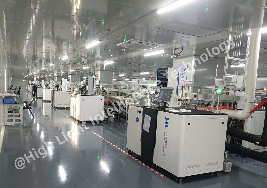
High Light Intelligence Technology, a pioneer in the CVD diamond industry, has advanced MPCVD technology and CVD diamond production workshops. We focus on producing high-purity lab-grown diamonds for the jewelry industry, and at the same time create industrial-grade CVD diamond products, covering single crystals, polycrystalline, films and diamond surface metallization. We also provide 6kw/10kw/15kw MPCVD equipment to help customers in all aspects, from equipment to products, and then to all-round services, to create brilliance together.









-

CVD Single-Crystal Diamonds: An Analysis of the Complete Processing Workflow from Gas-Phase Deposition to Finished Diamond Chips
MPCVD (Microwave Plasma Chemical Vapor Deposition) technology is currently the core process for producing high-quality single-crystal diamond s. Thanks to its advantages of low defect rates, high purity, and controllable large dimensions, it is widely used in fields such as semiconductor heat dissipation, precision optics, and high-end sensors. The final quality of single-crystal diamond s depends on comprehensive process control throughout the entire workflow—from vapor deposition growth to pos
-
Single-Crystal or Polycrystalline Diamond — Which Has Greater Potential?
As diamond continues to enter industries such as semiconductors, thermal management, optics, high-power electronics, and precision machining, the requirements for diamond materials are also evolving.
-
Diamond Polishing and Grinding Processes: Core Challenges and Industry Hurdles
Diamond is often hailed as the “ultimate material” – ranking 10 on the Mohs hardness scale, boasting an ultra‑high thermal conductivity (~2,200 W/(m·K)), excellent chemical stability, and broad optical transparency. These properties make it irreplaceable in cutting‑edge applications such as semiconductor heat dissipation, high‑end optics, and quantum chips. Yet the paradox of “good materials are hard to process” is nowhere more evident than in diamond. From rough grinding for planarization to at
-
Single-Crystal vs Polycrystalline CVD Diamond: Process Difference Lies in Growth Logic, Not Equipment
The process difference between single crystal and polycrystalline CVD diamond lies not in equipment, but in growth logic. Single crystal and polycrystalline CVD diamond are two functional new materials with completely independent growth mechanisms, lattice structures and performance systems. Their process logic, product features and application boundaries diverge fundamentally from the very start of deposition and growth. Comparing or selecting materials without considering their underlying crys


