- 中文
- English
- Español
Wide application of High Light Intelligence Technology's CVD diamond polycrystalline products
2024-07-19 09:50:57
Click:
“
In recent years, with the rapid development of science and technology, diamond, as a high-performance material, has shown great application potential in many fields. As a leader in the field of diamond material production and research and development, High Light Intelligence Technology has successfully launched CVD diamond polycrystalline wafer based on MPCVD technology through independent research and development and innovation. These products have been widely used in the market and have won w
”
In recent years, with the rapid development of science and technology, diamond, as a high-performance material, has shown great application potential in many fields. As a leader in the field of diamond material production and research and development, High Light Intelligence Technology has successfully launched CVD diamond polycrystalline wafer based on MPCVD technology through independent research and development and innovation. These products have been widely used in the market and have won wide recognition in the industry for their unique advantages and characteristics.
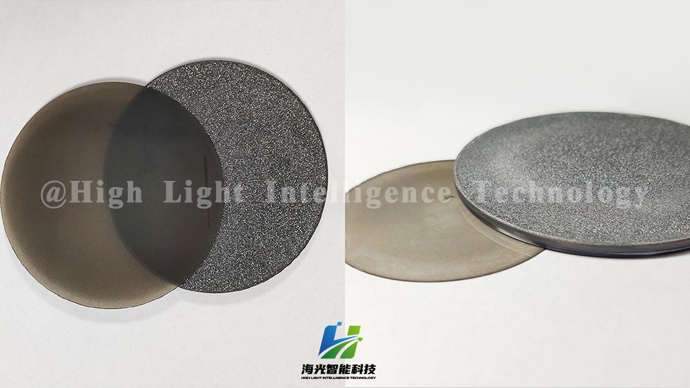
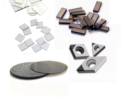
CVD diamond polycrystalline wafer are becoming increasingly important in high-tech and industrial fields due to their excellent performance and wide application. With technological progress and market growth, their application areas will continue to expand.
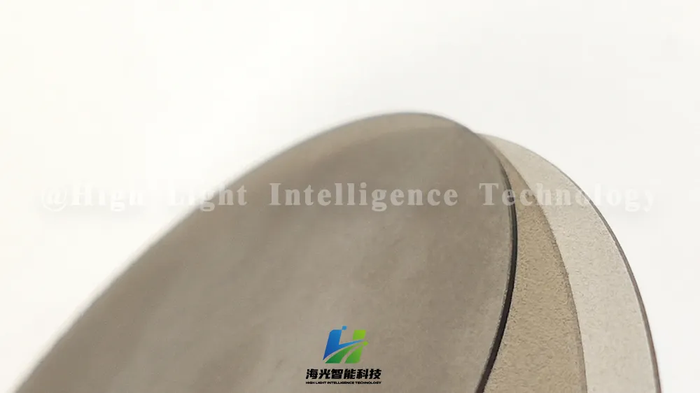
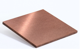
Advantage:
Excellent physical properties:
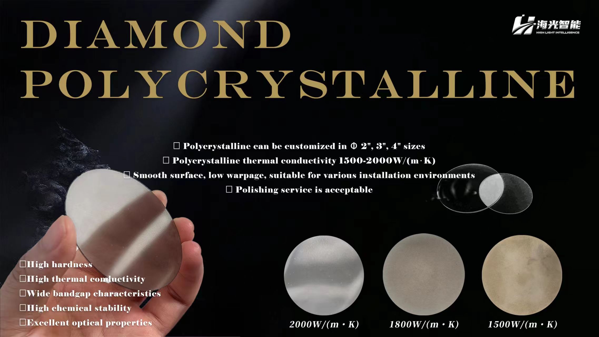
Top hardness, suitable for high-strength processing; extremely low thermal expansion coefficient, suitable for high-precision processing.
Excellent thermal conductivity:
The thermal conductivity is far higher than copper, which is the preferred material in the field of heat dissipation, ensuring stable operation of the equipment.
Wide-band high transmittance:
High transmittance from deep ultraviolet to far infrared, suitable for optical instruments and communication equipment.
Stable chemical properties:
Resistant to chemical corrosion, suitable for long-term use in harsh environments, stable and reliable performance.
Widely Used:
High-precision processing field
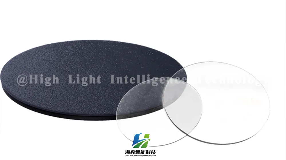
CVD diamond polycrystalline wafer have become an ideal choice in the field of high-precision processing due to their extremely high hardness and wear resistance. Whether it is wafer cutting in the semiconductor industry or precision parts processing in the aerospace field, diamond can provide excellent processing quality and efficiency.
Heat dissipation field
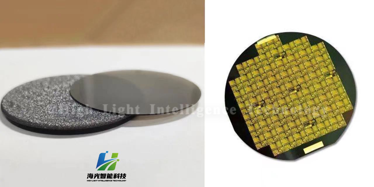
With the continuous development of electronic equipment, the problem of heat dissipation has become increasingly prominent. CVD diamond polycrystalline wafer have become a key material for solving heat dissipation problems with their excellent thermal conductivity. In applications such as CPU radiators and LED lamp heat sinks, diamond can quickly export heat to ensure the stable operation of the equipment.
Optical field
The wide-band high transmittance of CVD diamond polycrystalline wafer gives it a wide range of application prospects in the optical field. Whether it is the output window of a high-power laser or the protective window of an infrared detector, diamond can provide excellent optical performance to ensure the sensitivity and stability of the equipment.
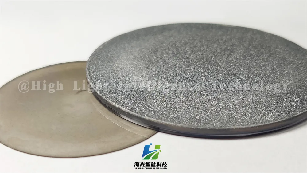
Through independent research and development and innovation, High Light Intelligence Technology has successfully launched diamond polycrystalline products based on MPCVD technology. These products have been widely used in many fields with their excellent physical properties, excellent thermal conductivity, wide-band high transmittance and stable chemical properties. In the future, with the continuous advancement of science and technology and the continuous expansion of the market, CVD diamond polycrystalline wafer will surely usher in a broader development prospect.









-

Single-Crystal vs Polycrystalline CVD Diamond: Process Difference Lies in Growth Logic, Not Equipment
The process difference between single crystal and polycrystalline CVD diamond lies not in equipment, but in growth logic. Single crystal and polycrystalline CVD diamond are two functional new materials with completely independent growth mechanisms, lattice structures and performance systems. Their process logic, product features and application boundaries diverge fundamentally from the very start of deposition and growth. Comparing or selecting materials without considering their underlying crys
-
From Lab-Grown Diamonds to Industrial Diamonds: Is It Time to Build an MPCVD Factory?
The lab-grown diamond industry is entering a new stage. Over the these few years, lab-grown diamonds have gradually gained wider acceptance in the jewelry market. With the development of production technology, equipment maturity and supply chain improvement, the industry is becoming more standardized and efficient. But beyond jewelry, another opportunity is attracting more attention:Industrial diamond applications.
-
Diamond‑Copper Composite: A Next‑Generation Solution for High‑Power Electronics Thermal Management
Diamond‑copper composite (DC) is an advanced metal‑matrix composite material consisting of diamond particles as the reinforcement phase and copper as the matrix, fabricated through state‑of‑the‑art composite preparation techniques. Diamond has the highest thermal conductivity of any naturally occurring material, with isotropic values ranging from 1200 to 2300 W/m·K. Copper, with a thermal conductivity of 401 W/m·K, ranks second only to silver among common metals. By combining the two, the compo
-
Mosaic Single‑Crystal Diamond: Breaking Size Limits
With an ultra‑wide bandgap of 5.47 eV, ultra‑high thermal conductivity (>2000 W/m·K), high carrier mobility (electron mobility up to 4500 cm²·V⁻¹·s⁻¹), and ultra‑high theoretical breakdown field strength (>10 MV/cm), Single‑Crystal Diamond (SCD) is an ideal candidate for next‑generation high‑power, high‑frequency and extreme‑environment electronic devices. However, both natural diamond and HPHT‑synthesized single‑crystal diamond are limited in lateral size, which greatly hinders large‑scal