

- 中文
- English
- Español
The journey of CVD rough diamond: from tiny beginnings to brilliant rough
2024-12-13 10:37:54
Click:
“
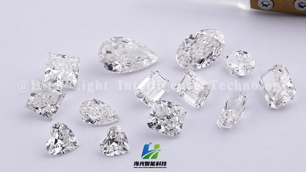
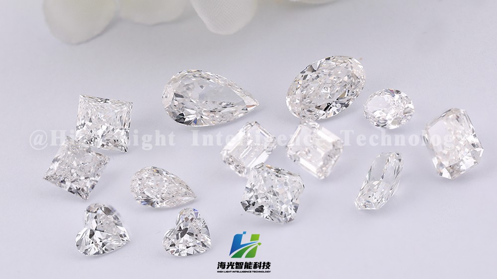
In the current era of rapid technological development, High Light Intelligence Technology has promoted the CVD diamond industry with its excellent technology and innovative spirit. It grows diamond materials from tiny starting points and transforms them into dazzling diamond roughs through independent research and development.
”
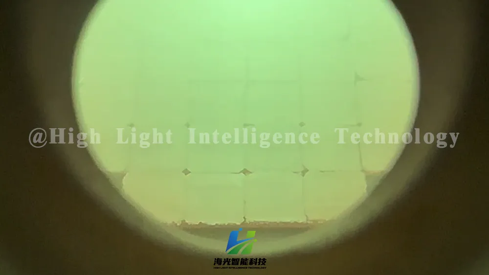
In the current era of rapid technological development, High Light Intelligence Technology has promoted the CVD diamond industry with its excellent technology and innovative spirit. It grows diamond materials from tiny starting points and transforms them into dazzling diamond roughs through independent research and development.
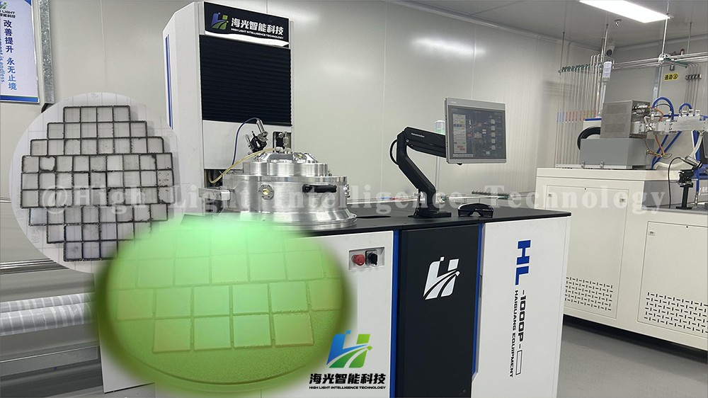
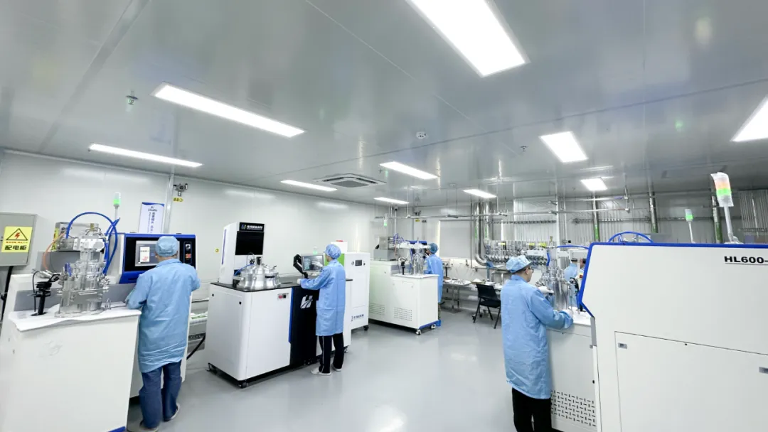
In our 100,000-class dust-free workshop, High Light Intelligence Technology's CVD diamond growth process is being carried out in our self-developed MPCVD technology. This magical process begins with a tiny CVD seed. When it is placed in the self-developed MPCVD machine, the real "transformation" begins.
MPCVD equipment precisely controls the gas environment (such as hydrogen, methane and other mixed gases), and under the excitation of microwave plasma, carbon atoms are induced to deposit on diamond seeds, slowly wrapping and gradually building up shining diamonds. This process is not only a perfect fusion of physics and chemistry, but also the ultimate pursuit of precise control technology by High Light Intelligence Technology.
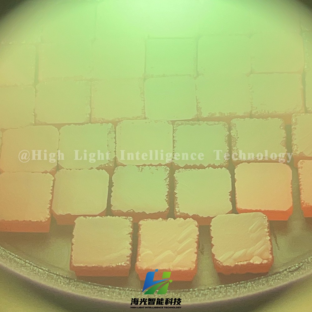
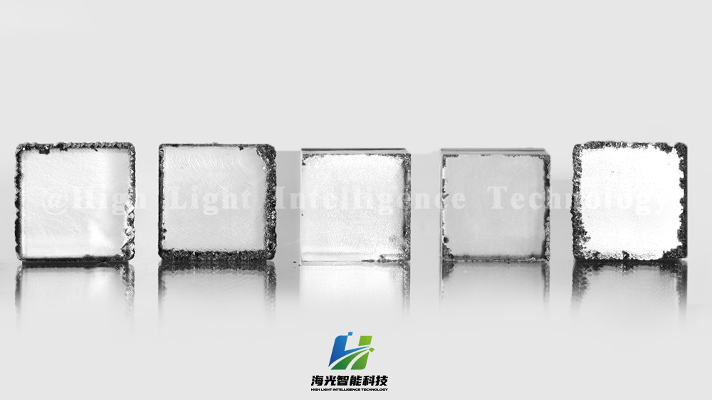
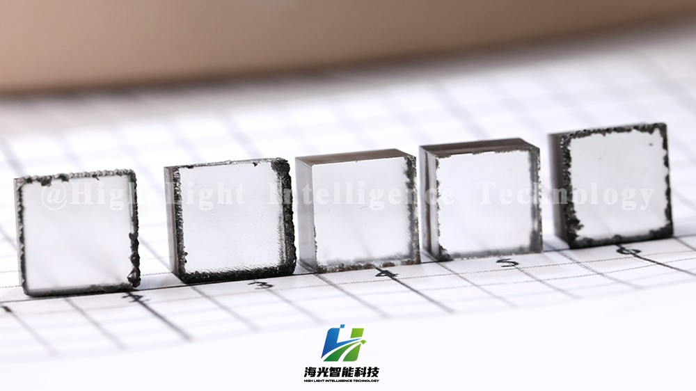
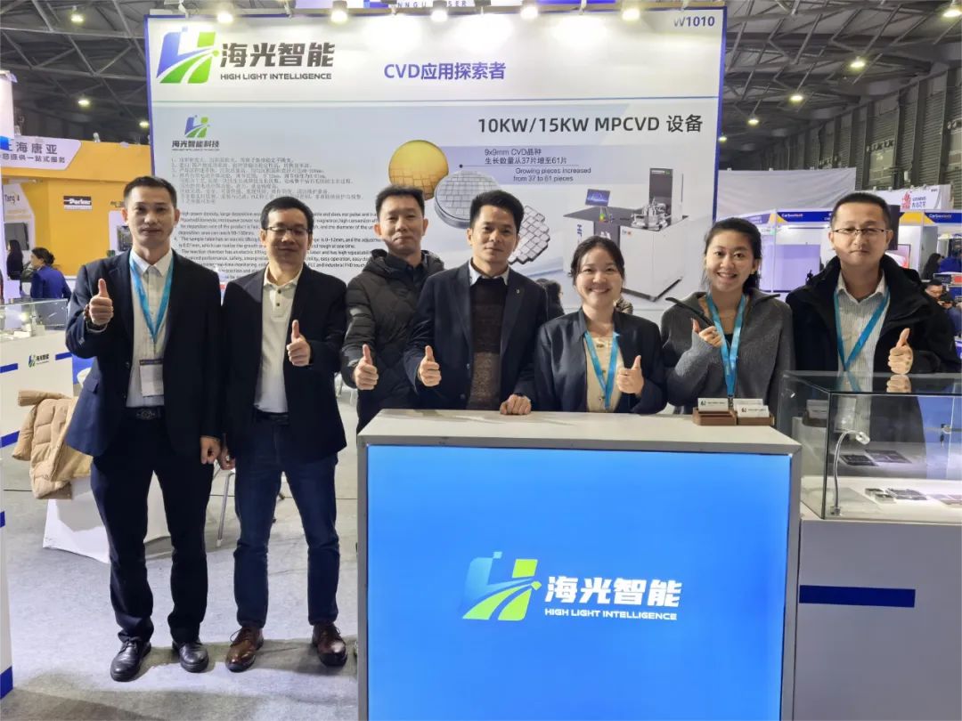
After the upgrade of High Light Intelligence Technology's MPCVD equipment, the number of 9x9mm CVD seed crystals grown has increased to a maximum of 61 pieces, with a monthly production capacity of approximately 345 carats, focusing on growing DEFG color and VVS-VS clarity diamond roughs. The yield rate has increased from 70% to 80%.









-

Foshan Highlight Intelligent Technology invites you to the 140th Canton Fair—join us at Booth 21.2A23-24 in the Friendship Hall to share in the brilliance.
Foshan Highlight Intelligent Technology invites you to the 140th Canton Fair—join us at Booth 21.2A23-24 in the Friendship Hall to share in the brilliance.
-
CVD Single-Crystal Diamonds: An Analysis of the Complete Processing Workflow from Gas-Phase Deposition to Finished Diamond Chips
MPCVD (Microwave Plasma Chemical Vapor Deposition) technology is currently the core process for producing high-quality single-crystal diamond s. Thanks to its advantages of low defect rates, high purity, and controllable large dimensions, it is widely used in fields such as semiconductor heat dissipation, precision optics, and high-end sensors. The final quality of single-crystal diamond s depends on comprehensive process control throughout the entire workflow—from vapor deposition growth to pos
-
Single-Crystal or Polycrystalline Diamond — Which Has Greater Potential?
As diamond continues to enter industries such as semiconductors, thermal management, optics, high-power electronics, and precision machining, the requirements for diamond materials are also evolving.
-
Diamond Polishing and Grinding Processes: Core Challenges and Industry Hurdles
Diamond is often hailed as the “ultimate material” – ranking 10 on the Mohs hardness scale, boasting an ultra‑high thermal conductivity (~2,200 W/(m·K)), excellent chemical stability, and broad optical transparency. These properties make it irreplaceable in cutting‑edge applications such as semiconductor heat dissipation, high‑end optics, and quantum chips. Yet the paradox of “good materials are hard to process” is nowhere more evident than in diamond. From rough grinding for planarization to at




