- 中文
- English
- Español
Diamond chip ampere-level switch verification is imminent!
2025-04-01 09:06:57
Click:
“
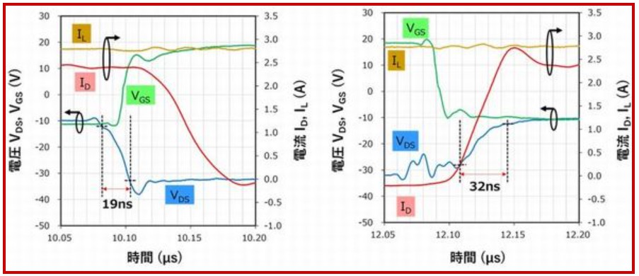
The National Institute of Advanced Industrial Science and Technology (AIST) in Japan, in collaboration with Honda R&D, has fabricated a prototype of a p-type diamond MOSFET and demonstrated ampere-level high-speed switching operation for the first time. In the future, the company plans to incorporate this technology into the next generation of mobile power devices and conduct operational verification in the hope of implementing it in society.
”

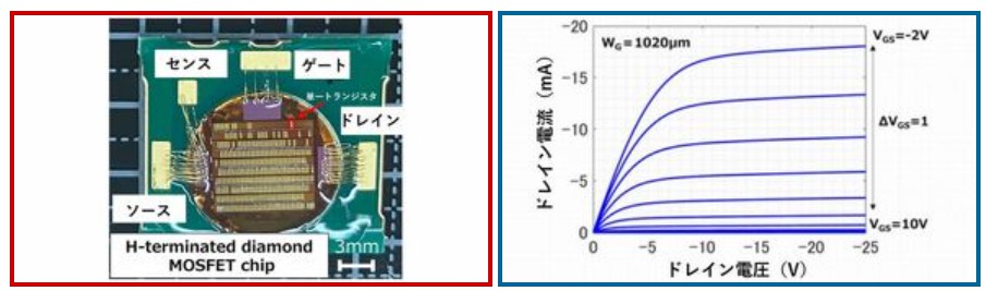
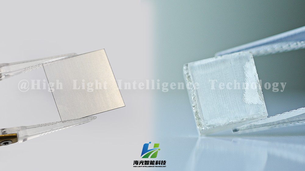
The research team increased the size of the substrate and developed parallel wiring technology to increase the current. They made a large number of p-type MOSFETs on a half-inch diamond substrate and evaluated their characteristics after wiring in parallel. They confirmed that the performance of the 1020μm gate width device was excellent and the substrate device manufacturing yield was high.
High Light Intelligence Technology, a pioneer in the CVD diamond industry, has advanced MPCVD technology and CVD diamond production workshops. We focus on producing high-purity lab-grown diamonds for the jewelry industry, and at the same time create industrial-grade CVD diamond products, covering single crystals, polycrystalline, films and diamond surface metallization and so on. We also provide 6kw/10kw/15kw MPCVD equipment to help customers in all aspects, from equipment to products, and then to all-round services, to create brilliance together.
*The articles and pictures are only for industry communication and sharing. If there is any infringement, please contact us to delete them.









-

Single-Crystal vs Polycrystalline CVD Diamond: Process Difference Lies in Growth Logic, Not Equipment
The process difference between single crystal and polycrystalline CVD diamond lies not in equipment, but in growth logic. Single crystal and polycrystalline CVD diamond are two functional new materials with completely independent growth mechanisms, lattice structures and performance systems. Their process logic, product features and application boundaries diverge fundamentally from the very start of deposition and growth. Comparing or selecting materials without considering their underlying crys
-
From Lab-Grown Diamonds to Industrial Diamonds: Is It Time to Build an MPCVD Factory?
The lab-grown diamond industry is entering a new stage. Over the these few years, lab-grown diamonds have gradually gained wider acceptance in the jewelry market. With the development of production technology, equipment maturity and supply chain improvement, the industry is becoming more standardized and efficient. But beyond jewelry, another opportunity is attracting more attention:Industrial diamond applications.
-
Diamond‑Copper Composite: A Next‑Generation Solution for High‑Power Electronics Thermal Management
Diamond‑copper composite (DC) is an advanced metal‑matrix composite material consisting of diamond particles as the reinforcement phase and copper as the matrix, fabricated through state‑of‑the‑art composite preparation techniques. Diamond has the highest thermal conductivity of any naturally occurring material, with isotropic values ranging from 1200 to 2300 W/m·K. Copper, with a thermal conductivity of 401 W/m·K, ranks second only to silver among common metals. By combining the two, the compo
-
Mosaic Single‑Crystal Diamond: Breaking Size Limits
With an ultra‑wide bandgap of 5.47 eV, ultra‑high thermal conductivity (>2000 W/m·K), high carrier mobility (electron mobility up to 4500 cm²·V⁻¹·s⁻¹), and ultra‑high theoretical breakdown field strength (>10 MV/cm), Single‑Crystal Diamond (SCD) is an ideal candidate for next‑generation high‑power, high‑frequency and extreme‑environment electronic devices. However, both natural diamond and HPHT‑synthesized single‑crystal diamond are limited in lateral size, which greatly hinders large‑scal