

- 中文
- English
- Español
GaN-on-diamond technology opens a new era of power device heat dissipation
2025-05-07 09:12:54
Click:
“
Recently, Liu Xinke's team from Shenzhen University published a review article 'GaN-on-diamond technology for next-generation power devices' in the English journal MaM. The article, with Fan Kangkai as the first author and Liu Xinke as the corresponding author, details the application of GaN-on-diamond technology in next-generation power devices, and systematically introduces its research status, key technologies and application prospects.
”

The consumer electronics industry is developing rapidly, and electronic devices are entering the era of high frequency and high power. Gallium nitride (GaN)-based power devices have become a popular choice for the next generation due to their excellent characteristics such as high breakdown field strength. However, when running at high power, the internal heat is difficult to dissipate, and the self-heating effect is significant, which will reduce performance and reliability. Traditional heat dissipation solutions, such as silicon or silicon carbide substrates, have limited thermal conductivity and are difficult to meet heat dissipation requirements, making the output power density of commercial GaN HEMTs far lower than the theoretical value. The industry urgently needs innovative heat dissipation solutions.

GaN-on-diamond technology combines GaN devices with diamond substrates with high thermal conductivity (2200 W/m/K) to improve the heat dissipation capacity of chips and solve the heat dissipation problem of GaN devices. Its integration methods include bonding and epitaxial growth. Studies have shown that the interface thermal resistance can be as low as 3 m²K/GW. This technology has great potential. It can conduct heat more efficiently, reduce operating temperature, increase power density, meet high power requirements, and promote the development of new technologies such as patterned growth, providing a new path for optimizing heat dissipation and improving device performance and reliability.


Thermal interface resistance (TBR) is a phenomenon in which heat transfer in electronic devices is blocked at the interface. It is mainly caused by the mismatch of atomic vibrations at the interface. It is affected by factors such as interface defects, integrity, and roughness. Defects can cause phonon scattering and increase thermal resistance. Reducing thermal interface resistance is the key to improving the heat dissipation performance of GaN-on-diamond. It can be achieved by optimizing bonding and epitaxial growth technology, such as using surface activated bonding technology. Selecting a suitable dielectric layer (such as SiNx) can also effectively reduce thermal resistance, highlighting the importance of dielectric layer selection for heat conduction.


There are currently four diamond-based heat dissipation technologies: polycrystalline and single-crystal diamond heat dissipation technologies, which use the characteristics of polycrystalline and single crystal to improve heat dissipation respectively; embedded diamond heat dissipation column technology to enhance local heat dissipation; diamond passivation layer technology has both protection and heat dissipation functions. GaN-on-diamond technology has great potential, but practical applications face challenges, such as the difficulty of diamond processing and preparation, the large difference in thermal expansion coefficients between GaN and diamond, which can easily lead to interface defects, and the technical difficulties of high-quality epitaxial layer stripping and diamond substrate growth.

The interfacial thermal resistance is closely related to the electron-phonon coupling theory, which refers to the interaction between electrons and lattice vibrations. In the GaN-on-diamond system, it has a significant impact on interfacial heat transfer. It can not only promote the energy exchange between electrons and lattices, affecting heat transfer, but also increase the interfacial thermal resistance by distorting the lattice vibration, hindering heat transfer. In order to accurately calculate and measure the interfacial thermal resistance, a variety of calculation methods such as the diffuse reflection mismatch model and experimental measurement methods such as the time-domain thermal reflection method are proposed to provide theoretical support for optimizing the heat dissipation performance of the device.

GaN-on-diamond technology has broad prospects in the fields of RF, power and microwave devices, and is expected to promote the leap in performance, reliability and life of GaN devices, and may be expanded to the field of ultra-wide bandgap semiconductors in the future. However, its large-scale commercial application faces technical and engineering challenges, such as optimizing the bonding process and solving lattice mismatch. Future research will focus on reducing interface thermal resistance, developing efficient heat dissipation packaging technology, and exploring new material combinations. This technology is very promising and is attracting attention, and is expected to become a new engine for the development of the semiconductor industry.

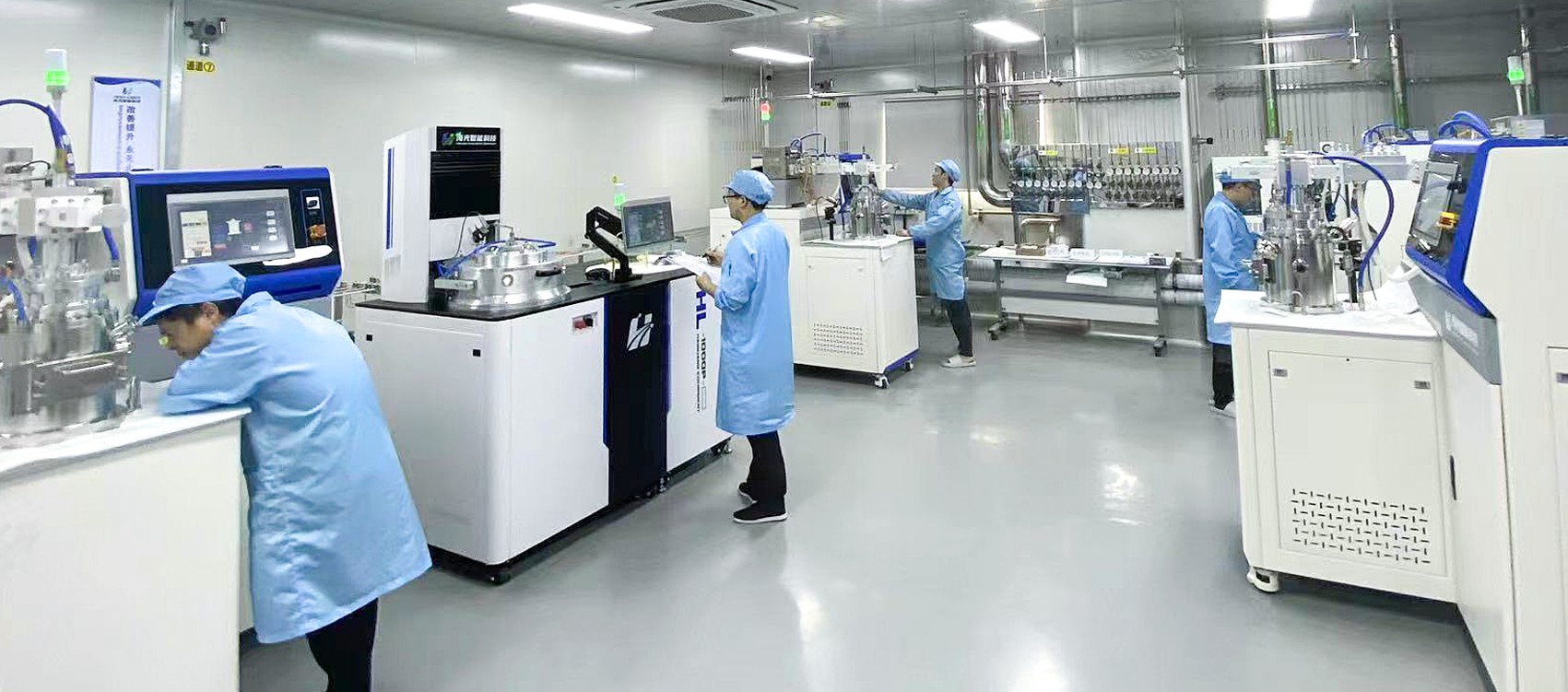
High Light Intelligence Technology, a pioneer in the CVD diamond industry, has advanced MPCVD technology and CVD diamond production workshops. We focus on producing high-purity lab-grown diamonds for the jewelry industry, and at the same time create industrial-grade CVD diamond products, covering single crystals, polycrystalline, films and diamond surface metallization and so on. We also provide 6kw/10kw/15kw MPCVD equipment to help customers in all aspects, from equipment to products, and then to all-round services, to create brilliance together.
*The articles and pictures are only for industry communication and sharing. If there is any infringement, please contact us to delete them.









-

Foshan Highlight Intelligent Technology invites you to the 140th Canton Fair—join us at Booth 21.2A23-24 in the Friendship Hall to share in the brilliance.
Foshan Highlight Intelligent Technology invites you to the 140th Canton Fair—join us at Booth 21.2A23-24 in the Friendship Hall to share in the brilliance.
-
CVD Single-Crystal Diamonds: An Analysis of the Complete Processing Workflow from Gas-Phase Deposition to Finished Diamond Chips
MPCVD (Microwave Plasma Chemical Vapor Deposition) technology is currently the core process for producing high-quality single-crystal diamond s. Thanks to its advantages of low defect rates, high purity, and controllable large dimensions, it is widely used in fields such as semiconductor heat dissipation, precision optics, and high-end sensors. The final quality of single-crystal diamond s depends on comprehensive process control throughout the entire workflow—from vapor deposition growth to pos
-
Single-Crystal or Polycrystalline Diamond — Which Has Greater Potential?
As diamond continues to enter industries such as semiconductors, thermal management, optics, high-power electronics, and precision machining, the requirements for diamond materials are also evolving.
-
Diamond Polishing and Grinding Processes: Core Challenges and Industry Hurdles
Diamond is often hailed as the “ultimate material” – ranking 10 on the Mohs hardness scale, boasting an ultra‑high thermal conductivity (~2,200 W/(m·K)), excellent chemical stability, and broad optical transparency. These properties make it irreplaceable in cutting‑edge applications such as semiconductor heat dissipation, high‑end optics, and quantum chips. Yet the paradox of “good materials are hard to process” is nowhere more evident than in diamond. From rough grinding for planarization to at




