

- 中文
- English
- Español
CVD Diamond: Growing Diamonds for the Future
2026-08-21 16:42:31
Click:
“
When people talk about diamonds, the first thing that comes to mind is usually luxury jewelry.
But today, diamond is becoming much more than a gemstone.
With the rapid development of AI, semiconductors, 5G, and high-power electronics, diamond is attracting attention as an advanced material because of its exceptional thermal properties.
”
When people talk about diamonds, the first thing that comes to mind is usually luxury jewelry.
But today, diamond is becoming much more than a gemstone.
With the rapid development of AI, semiconductors, 5G, and high-power electronics, diamond is attracting attention as an advanced material because of its exceptional thermal properties.
What is CVD Diamond?
CVD stands for Chemical Vapor Deposition.
Unlike natural diamonds that grow underground over millions of years, CVD diamonds are grown in a controlled environment by depositing carbon atoms layer by layer onto a diamond seed
Simply explained:
Natural diamond is created by nature over millions of years.
CVD diamond is grown atom by atom through advanced technology.
CVD technology allows manufacturers to control:
· Size
· Purity
· Defect level
· Thermal performance
Common CVD Diamond Growth Technologies
There are several CVD methods, but the two most commonly discussed technologies for diamond growth are:
1. MPCVD (Microwave Plasma Chemical Vapor Deposition)
2. HFCVD (Hot Filament Chemical Vapor Deposition)
Although both use carbon-containing gases to grow diamond, their growth mechanisms and applications are different.
Ⅰ. MPCVD Diamond
How does it work?
MPCVD uses microwave energy to generate plasma, activating methane (CH₄) and hydrogen (H₂) to grow diamond on a seed crystal.
Advantages of MPCVD
1. Higher Purity and Better Crystal Quality
MPCVD does not require electrodes inside the reaction chamber, which helps reduce contamination and improves diamond purity.
This makes it suitable for applications where material quality is critical.
2. Excellent Thermal Conductivity
High-quality MPCVD diamond can achieve thermal conductivity of:
1500–2200 W/m·K
This makes it ideal for:
· Semiconductor heat spreaders
· GaN power devices
· RF electronics
· Advanced thermal management systems
3. Better Capability for High-Quality Large Diamond Growth
MPCVD is widely used for:
· Single crystal diamond
· High-performance diamond wafers
Typical sizes include:
· 10 × 10 mm
· 20 × 20 mm
· 30 × 30 mm and beyond
The challenge is not only growing larger diamonds, but maintaining high purity, low defects, and stable performance.
Ⅱ. HFCVD Diamond
How does it work?
HFCVD uses high-temperature filaments to activate carbon-containing gases and deposit diamond.
Advantages of HFCVD
1. Lower Equipment Cost
Compared with MPCVD, HFCVD has a simpler structure and lower initial investment.
2. One advantage of HFCVD that cannot be ignored is its ability to achieve large-area diamond deposition.
By using multiple filament arrangements, HFCVD can cover larger surfaces and is suitable for large-area coatings.
HFCVD is widely used for:
· Cutting tools
· Wear-resistant coatings
· Industrial diamond films
It is a mature technology for surface protection and industrial applications.
Limitations of HFCVD
1. Lower Thermal Performance
Typical thermal conductivity:
500–1200 W/m·K
Compared with MPCVD, HFCVD diamond usually has:
· Higher defect density
· Higher contamination risk
· More limitations for electronic-grade applications
MPCVD vs HFCVD Comparison

From my perspective as a Project Manager in the diamond industry, choosing a CVD technology is not only about cost or production speed.
The key questions are:
· Can we achieve higher purity?
· Can we control defects?
· Can we maintain stable thermal performance?
· Does the material match the final application?
Different technologies serve different markets.
HFCVD focuses on cost-effective industrial applications.
MPCVD focuses on high-performance diamond materials for future technologies.
I believe CVD diamond is one of the bridges connecting traditional diamond craftsmanship with future technology.
What application do you think will create the biggest opportunity for CVD diamond in the next decade?
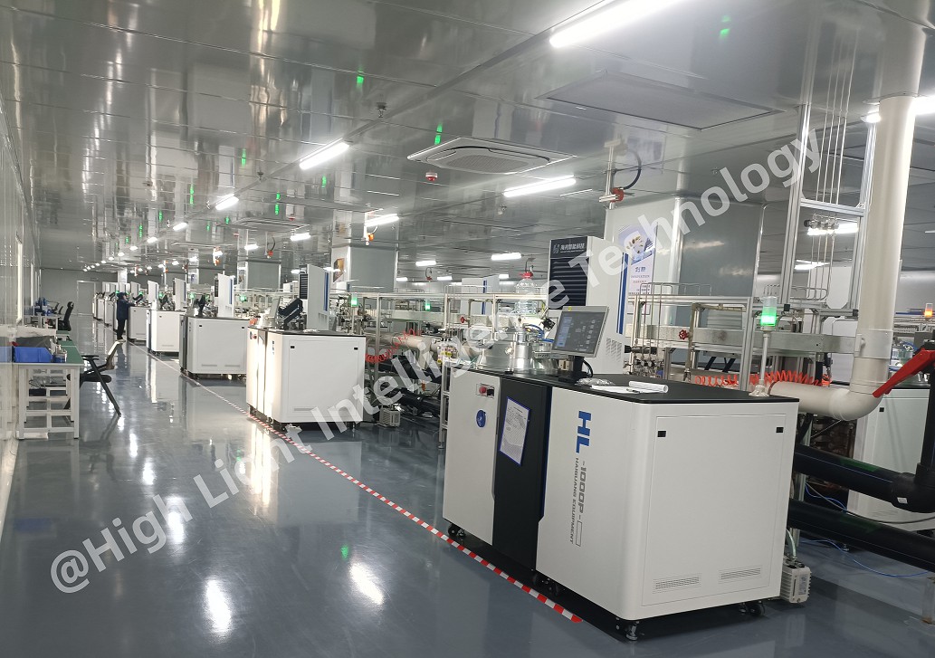
High Light Intelligence Technology, a pioneer in the CVD diamond industry, has advanced MPCVD technology and CVD diamond production workshops. We focus on producing high-purity lab-grown diamonds for the jewelry industry, and at the same time create industrial-grade CVD diamond products, covering single crystals, polycrystalline, films and diamond surface metallization. We also provide 6kw/10kw/15kw MPCVD equipment to help customers in all aspects, from equipment to products, and then to all-round services, to create brilliance together.









-

CVD Single-Crystal Diamonds: An Analysis of the Complete Processing Workflow from Gas-Phase Deposition to Finished Diamond Chips
MPCVD (Microwave Plasma Chemical Vapor Deposition) technology is currently the core process for producing high-quality single-crystal diamond s. Thanks to its advantages of low defect rates, high purity, and controllable large dimensions, it is widely used in fields such as semiconductor heat dissipation, precision optics, and high-end sensors. The final quality of single-crystal diamond s depends on comprehensive process control throughout the entire workflow—from vapor deposition growth to pos
-
Single-Crystal or Polycrystalline Diamond — Which Has Greater Potential?
As diamond continues to enter industries such as semiconductors, thermal management, optics, high-power electronics, and precision machining, the requirements for diamond materials are also evolving.
-
Diamond Polishing and Grinding Processes: Core Challenges and Industry Hurdles
Diamond is often hailed as the “ultimate material” – ranking 10 on the Mohs hardness scale, boasting an ultra‑high thermal conductivity (~2,200 W/(m·K)), excellent chemical stability, and broad optical transparency. These properties make it irreplaceable in cutting‑edge applications such as semiconductor heat dissipation, high‑end optics, and quantum chips. Yet the paradox of “good materials are hard to process” is nowhere more evident than in diamond. From rough grinding for planarization to at
-
Single-Crystal vs Polycrystalline CVD Diamond: Process Difference Lies in Growth Logic, Not Equipment
The process difference between single crystal and polycrystalline CVD diamond lies not in equipment, but in growth logic. Single crystal and polycrystalline CVD diamond are two functional new materials with completely independent growth mechanisms, lattice structures and performance systems. Their process logic, product features and application boundaries diverge fundamentally from the very start of deposition and growth. Comparing or selecting materials without considering their underlying crys




