

- 中文
- English
- Español
CVD Seed Crystals: The “Core Foundation” of the Synthetic Diamond Industry
2026-01-07 10:04:37
Click:
“
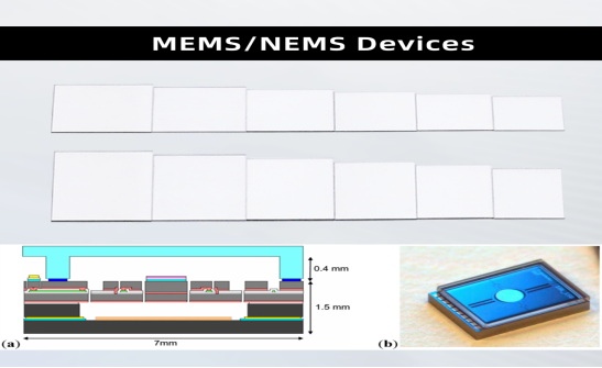
With the development of semiconductor technology, the improvement of chip performance poses a significant challenge to heat dissipation. Moore's Law is slowing down, and the process is approaching its limit. Advanced packaging is the key to continuing the performance improvement.
”
What are CVD seed ? Simply put, they serve as the “seed” substrate guiding the epitaxial growth of diamond crystals during the chemical vapor deposition (CVD) process for producing synthetic diamonds. Serving as the core reference for diamond growth, CVD seeds are typically precision-machined from high-quality natural diamonds or high-pressure high-temperature (HPHT) synthetic diamonds. They provide a stable crystallographic template for subsequent crystal growth, with their quality directly determining the performance and quality of the final diamond product. As such, they represent the foundational critical material at the origin of the synthetic diamond supply chain.
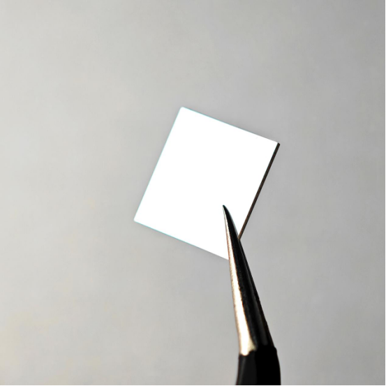
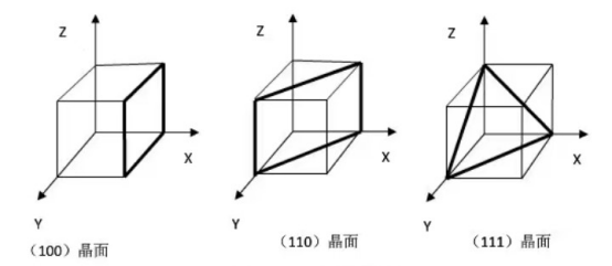
Crystal orientation is the core critical attribute of CVD seeds, referring to the direction of atomic arrangement within the crystal. It plays a decisive role in determining the growth morphology and properties of the diamond. CVD seed crystals exhibit crystal orientations of (100), (110), and (111), each suited for distinct applications: (100) and (110) orientations are used for growing jewelry-grade rough diamonds, while industrial single crystals require no specific orientation.
The production of high-quality CVD seed crystals involves extremely high barriers, requiring multiple precise and stringent process steps. The core workflow comprises three stages. The first step is raw material selection, prioritizing natural diamonds or high-pressure high-temperature (HPHT) synthetic diamonds with high purity and minimal defects as substrates—this is fundamental to ensuring the seed crystal's baseline quality. The second step involves directional machining. Through precision techniques like laser cutting and grinding, the substrate is processed into predetermined dimensions—currently, mainstream industrial-grade CVD seed crystals measure 5-15mm square. Producing oversized crystals (20mm+) is a key technical challenge in large-diamond fabrication. Precise control of crystal orientation during this stage is crucial to prevent growth defects later. The third step involves fine polishing and inspection. The processed seed crystal undergoes nanoscale polishing to ensure surface roughness meets standards, preventing interference with epitaxial growth. Subsequently, specialized inspection equipment is used for impurity detection and crystal orientation calibration. Furthermore, thickness control is critical, with conventional thicknesses ranging from 0.3 to 0.6mm, balancing support strength during growth and allowing sufficient allowance for subsequent processing.
CVD seed crystals exhibit highly specialized applications across artificial diamond segments, demonstrating a “tiered adaptation” characteristic. In industrial processing, seeds for manufacturing diamond cutting and grinding tools prioritize dimensional stability with relatively relaxed purity requirements. In electronics, seeds for producing heat sinks and semiconductor substrates demand high purity and low defect levels to guarantee exceptional thermal conductivity and semiconductor performance, supporting advanced devices like SiC/GaN power modules and AI chips. In the jewelry sector, seed crystals for cultivated diamonds pursue crystal integrity and optical purity to ensure finished products exhibit exceptional fire and clarity.
As demand for high-performance diamonds surges in advanced fields like new energy and semiconductors, CVD seeds are evolving toward larger dimensions, higher precision, and lower costs, continuously supporting the high-quality development of the synthetic diamond industry.
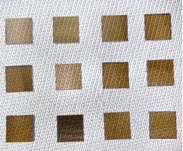
Foshan High Light Intelligence offers CVD seed in a full size range from 7-25mm, with thicknesses between 0.3-0.5mm. These are categorized into two major types based on crystal orientation: 100-type seeds support multi-directional growth on all sides and the front face, while 110-type seeds allow growth only on the front face, catering to diverse production requirements.
Quality control is stringent, employing dual inspection via metallurgical microscopes and polarizing microscopes to ensure no impurities, no edge defects, positive dimensional tolerances, and uniform stress distribution at 50x magnification. Supply options are flexible: smaller 7-9mm sizes undergo single-sided polishing for easier handling and inspection, while industrial-grade products can be customized to order. With comprehensive size coverage, premium quality standards, and flexible supply capabilities, High Light CVD seed crystals provide stable, reliable substrate support for lab-grown diamond enterprises, enabling efficient production of diverse high-quality lab-grown diamonds.
High Light Intelligence Technology, a pioneer in the CVD diamond industry, has advanced MPCVD technology and CVD diamond production workshops. We focus on producing high-purity lab-grown diamonds for the jewelry industry, and at the same time create industrial-grade CVD diamond products, covering single crystals, polycrystalline, films and diamond surface metallization. We also provide 6kw/10kw/15kw MPCVD equipment to help customers in all aspects, from equipment to products, and then to all-round services, to create brilliance together.


-

Z-Axis System: The Key to Stable Production of MPCVD Diamonds
Microwave Plasma Chemical Vapor Deposition is the mainstream method for producing high-quality diamonds in the industry. When the equipment is running, it first pumps the reaction chamber into a vacuum state to strictly ensure the chamber is fully sealed and airtight. Then, the microwave device releases energy, and special mixed reaction gases are fed into the chamber. Under the action of energy, a stable plasma area is formed. These highly active plasmas provide stable heat and reaction conditi
-
How to Choose the Right MPCVD Equipment?
MPCVD equipment is a critical asset across a wide range of industries, including industrial manufacturing, semiconductor thermal management, precision cutting tools, and lab-grown diamonds. Choosing the right equipment not only boosts production efficiency and ensures consistent product quality but also effectively controls long-term costs, making your entire production process smoother and more competitive. Many people struggle with the question: How do I make the right choice? Today, drawing o
-
CVD Diamond Clarity: How to Avoid Inclusions That Affect Jewelry Value
After selecting a loose diamond, the setting not only determines the diamond’s security but also directly affects its perceived size. With diamonds of the same weight, choosing the right setting design can effortlessly create the surprise of “small carats making a big impact,” saving on your budget while enhancing the diamond’s quality. Among these, pavé and prong settings are the two most classic and effective ways to make a diamond appear larger. Paired with specialized designs that maximize t
-
How Diamond Became the Ultimate Thermal Solution in the Era of Computing Power
The iconic narrative behind the legendary "A Diamond is Forever" slogan has long been upended by China's industrial prowess. Once synonymous with luxury and rarity, this gem has shed its glamorous aura to become an indispensable thermal management material for high-power devices. In an era of explosive growth in AI computing power, it has taken up the mantle of "cooling to save computing power".


