- 中文
- English
- Español
Diamond‑Copper Composite: A Next‑Generation Solution for High‑Power Electronics Thermal Management
2026-09-14 15:00:45
Click:
“
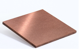
Diamond‑copper composite (DC) is an advanced metal‑matrix composite material consisting of diamond particles as the reinforcement phase and copper as the matrix, fabricated through state‑of‑the‑art composite preparation techniques.
Diamond has the highest thermal conductivity of any naturally occurring material, with isotropic values ranging from 1200 to 2300 W/m·K. Copper, with a thermal conductivity of 401 W/m·K, ranks second only to silver among common metals. By combining the two, the compo
”
Diamond‑copper composite (DC) is an advanced metal‑matrix composite material consisting of diamond particles as the reinforcement phase and copper as the matrix, fabricated through state‑of‑the‑art composite preparation techniques.
Diamond has the highest thermal conductivity of any naturally occurring material, with isotropic values ranging from 1200 to 2300 W/m·K. Copper, with a thermal conductivity of 401 W/m·K, ranks second only to silver among common metals. By combining the two, the composite leverages diamond's ultra‑high heat conduction while retaining copper's good workability, making it an ideal material for thermal management in electronic packaging.
2.1 Ultra‑High Thermal Conductivity
Diamond‑copper composites exhibit thermal conductivity in the range of 600–800 W/m·K, far exceeding traditional metal‑based materials. Some high‑end products, through process optimization, can achieve conductivities exceeding 1000 W/m·K. Compared to pure copper (401 W/m·K), thermal performance improves by 50%–100%.
Research data show that with multi‑layer interface design, diamond/copper composites can reach 743 W/m·K. Using spark plasma sintering (SPS) at 1400 N sintering pressure and 900°C, the maximum thermal conductivity can reach 564.2 W/m·K. Diamond with optimized interfaces and surface treatment, after vacuum hot pressing with 50 vol% diamond content, yields composites with thermal conductivity up to 706 W/m·K.
2.2 Tunable Coefficient of Thermal Expansion (CTE)
One of the most outstanding advantages of diamond‑copper composites is that their CTE can be precisely tailored by adjusting the volume fraction of diamond and copper, as well as the interface structure.
Diamond has an extremely low CTE of approximately 1 ppm/K, while pure copper has a CTE of about 17 ppm/K. By controlling the ratio, the CTE of diamond‑copper composites can be accurately tuned to 5–7×10⁻⁶/K, closely matching semiconductor materials such as silicon (\3 ppm/K), gallium arsenide (\5.8 ppm/K), and silicon carbide (~4.0–4.5 ppm/K).
This property is critical for electronic packaging—poor CTE matching leads to solder cracking, interface delamination during thermal cycling, and ultimately chip failure.
2.3 Excellent Comprehensive Properties
Beyond thermal conductivity and CTE, diamond‑copper composites offer additional advantages:
• Light weight: Density is approximately 40% lower than that of tungsten‑copper alloys, meeting weight‑sensitive requirements in aerospace and other applications.
• High relative density: Advanced processes can achieve density above 99.9%.
• Good hermeticity: Surfaces can be plated with Ni/Au to enable hermetic packaging, with leak rates down to 10⁻⁹ Pa·m³/s.
• High interfacial bonding strength: Using magnetron sputtering combined with hot isostatic pressing, bonding strength can exceed 150 MPa.

The fabrication process directly affects final performance. Current mainstream processes include:
3.1 Spark Plasma Sintering (SPS)
SPS is a common technique for producing high‑performance diamond/copper composites. Optimal properties are achieved with 50 vol% diamond at a sintering pressure of 30 MPa, holding temperature of 900°C, and holding time of 20 minutes.
3.2 Powder Metallurgy (PM)
Traditional powder metallurgy is a classic method for preparing copper‑diamond composites, featuring mature technology and relatively low cost.
3.3 Friction Stir Processing (FSP)
This method achieves composite formation through intense plastic deformation, resulting in refined microstructures and good interfacial bonding.
3.4 Gas Pressure Infiltration
Liquid copper is infiltrated into a diamond preform under pressure, achieving near‑100% density. This approach enables near‑net shaping, requires minimal post‑machining, and is simple and reliable.
3.5 Interface Modification Techniques
The poor wettability and high interfacial thermal resistance between diamond and copper limit composite performance improvement. Current mainstream modification approaches include:
• Diamond surface coating: Coating diamond with a Cr‑B composite layer (thickness ~0.1–5 μm), followed by SPS or hot pressing with copper.
• Matrix alloying: Introducing elements such as boron powder to significantly improve interfacial bonding strength.
• Chromium plating modification: Surface‑chromium‑modified diamond particles are used with vacuum hot‑pressing sintering.

Thanks to high thermal conductivity and low CTE, diamond‑copper composites have been adopted in multiple high‑end fields:
4.1 AI Servers and GPU Cooling Modules
With the explosive growth in AI computing power, GPU and AI chip power consumption continues to rise, and traditional cooling materials are struggling to keep up. Diamond‑copper composites, with ultra‑high thermal conductivity of 600–800 W/m·K, can rapidly dissipate extreme heat fluxes.
4.2 IGBT Power Semiconductor Substrates
IGBT modules generate substantial heat during operation and must maintain reliability over a wide temperature range. The CTE of diamond‑copper composites can closely match semiconductor materials, effectively reducing thermal‑stress‑induced package failures.
4.3 High‑End CPU and Advanced Packaging Heat Sinks
In high‑end CPU and advanced packaging applications, heat flux densities can reach 1 kW/cm². Diamond‑copper composites enable “near‑junction cooling” to effectively lower junction temperatures.
4.4 SiC Power Modules
Silicon carbide (SiC) devices, with outstanding electrical and thermal properties, are becoming the core choice for high‑power‑density inverters. As device sizes shrink and power densities increase, packaging and heat dissipation have become critical bottlenecks. Diamond‑copper composites are emerging as an ideal internal cooling solution for SiC power modules.
4.5 Aerospace and Military Electronics
The density of diamond‑copper composites is about 40% lower than that of tungsten‑copper alloys, while offering excellent hermeticity and reliability—meeting the special requirements of aerospace for weight‑sensitive components.

Diamond‑copper composites combine ultra‑high thermal conductivity, tunable CTE, light weight, and high reliability, positioning them as a benchmark material in high‑power electronics thermal management. Whether for AI computing infrastructure, power semiconductor modules, advanced packaging, or aerospace applications, diamond‑copper demonstrates irreplaceable performance value.
If you are seeking a thermal solution with high conductivity, low expansion, and superior reliability, diamond‑copper composite is worth your in‑depth consideration.
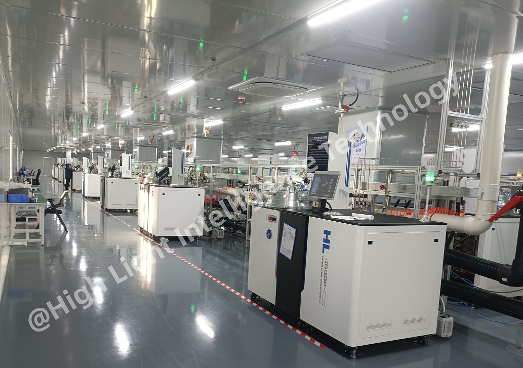
High Light Intelligence Technology, a pioneer in the CVD diamond industry, has advanced MPCVD technology and CVD diamond production workshops. We focus on producing high-purity lab-grown diamonds for the jewelry industry, and at the same time create industrial-grade CVD diamond products, covering single crystals, polycrystalline, films and diamond surface metallization. We also provide 6kw/10kw/15kw MPCVD equipment to help customers in all aspects, from equipment to products, and then to all-round services, to create brilliance together.









-

From Lab-Grown Diamonds to Industrial Diamonds: Is It Time to Build an MPCVD Factory?-副本
The lab-grown diamond industry is entering a new stage. Over the these few years, lab-grown diamonds have gradually gained wider acceptance in the jewelry market. With the development of production technology, equipment maturity and supply chain improvement, the industry is becoming more standardized and efficient. But beyond jewelry, another opportunity is attracting more attention:Industrial diamond applications.
-
From Lab-Grown Diamonds to Industrial Diamonds: Is It Time to Build an MPCVD Factory?
The lab-grown diamond industry is entering a new stage. Over the these few years, lab-grown diamonds have gradually gained wider acceptance in the jewelry market. With the development of production technology, equipment maturity and supply chain improvement, the industry is becoming more standardized and efficient. But beyond jewelry, another opportunity is attracting more attention:Industrial diamond applications.
-
Diamond‑Copper Composite: A Next‑Generation Solution for High‑Power Electronics Thermal Management
Diamond‑copper composite (DC) is an advanced metal‑matrix composite material consisting of diamond particles as the reinforcement phase and copper as the matrix, fabricated through state‑of‑the‑art composite preparation techniques. Diamond has the highest thermal conductivity of any naturally occurring material, with isotropic values ranging from 1200 to 2300 W/m·K. Copper, with a thermal conductivity of 401 W/m·K, ranks second only to silver among common metals. By combining the two, the compo
-
Mosaic Single‑Crystal Diamond: Breaking Size Limits
With an ultra‑wide bandgap of 5.47 eV, ultra‑high thermal conductivity (>2000 W/m·K), high carrier mobility (electron mobility up to 4500 cm²·V⁻¹·s⁻¹), and ultra‑high theoretical breakdown field strength (>10 MV/cm), Single‑Crystal Diamond (SCD) is an ideal candidate for next‑generation high‑power, high‑frequency and extreme‑environment electronic devices. However, both natural diamond and HPHT‑synthesized single‑crystal diamond are limited in lateral size, which greatly hinders large‑scal