

- 中文
- English
- Español
How to Visually Measure the Table Aspect Ratio of a Diamond
2023-05-16 20:22:33
Click:
“
The mesa diameter is defined as the inner diagonal of a regular octagon. Estimate the ratio of half of the inner diagonal to the girdle radius to determine the table width ratio.
”
There are two commonly used methods for visually estimating the station width ratio.
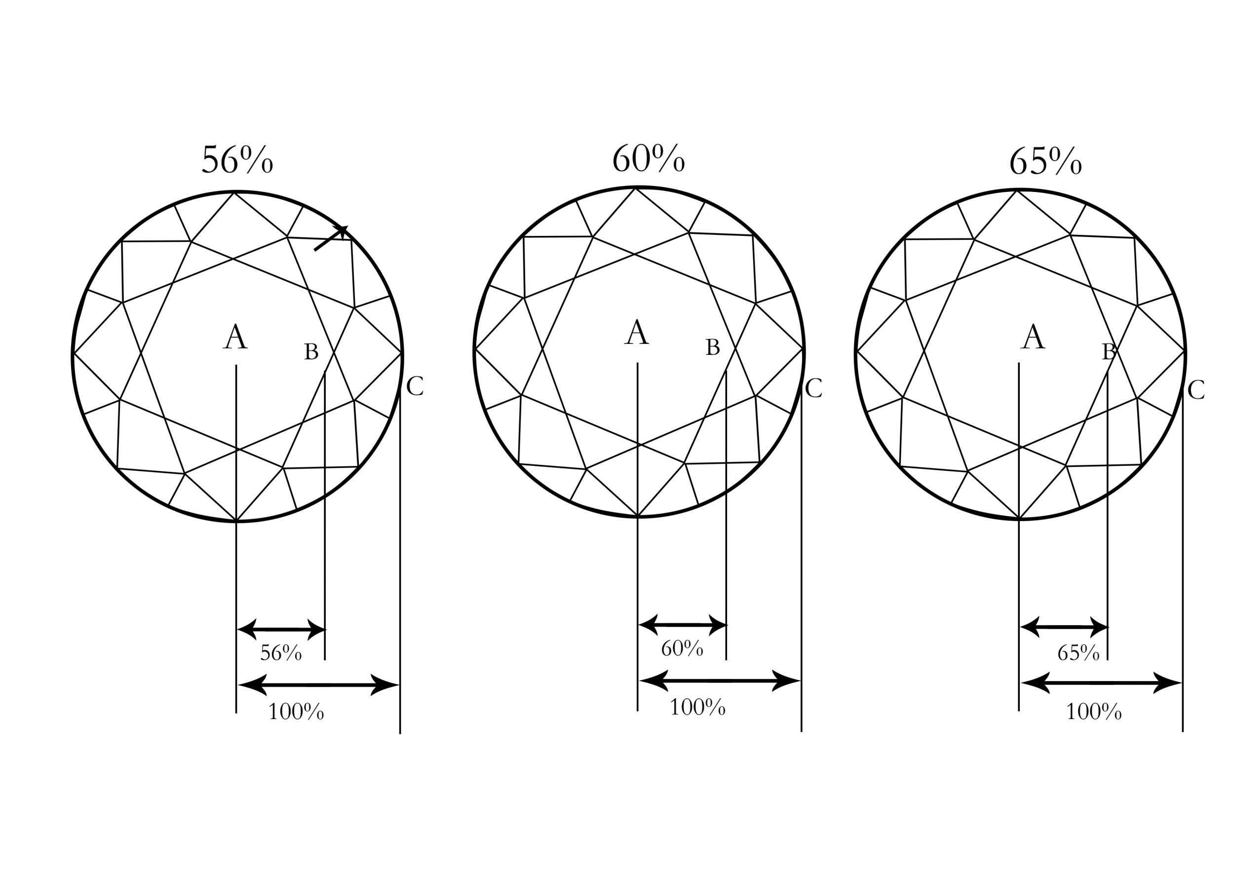
1. Ratio method (direct estimation method) The mesa diameter is defined as the inner diagonal of a regular octagon. Estimate the ratio of half of the inner diagonal to the girdle radius to determine the table width ratio.
The specific steps are: the line of sight is perpendicular to the table, and the three points A, B, and C in the figure are connected by an imaginary straight line, and the value of AB:BC is visually measured, which is the table width ratio.
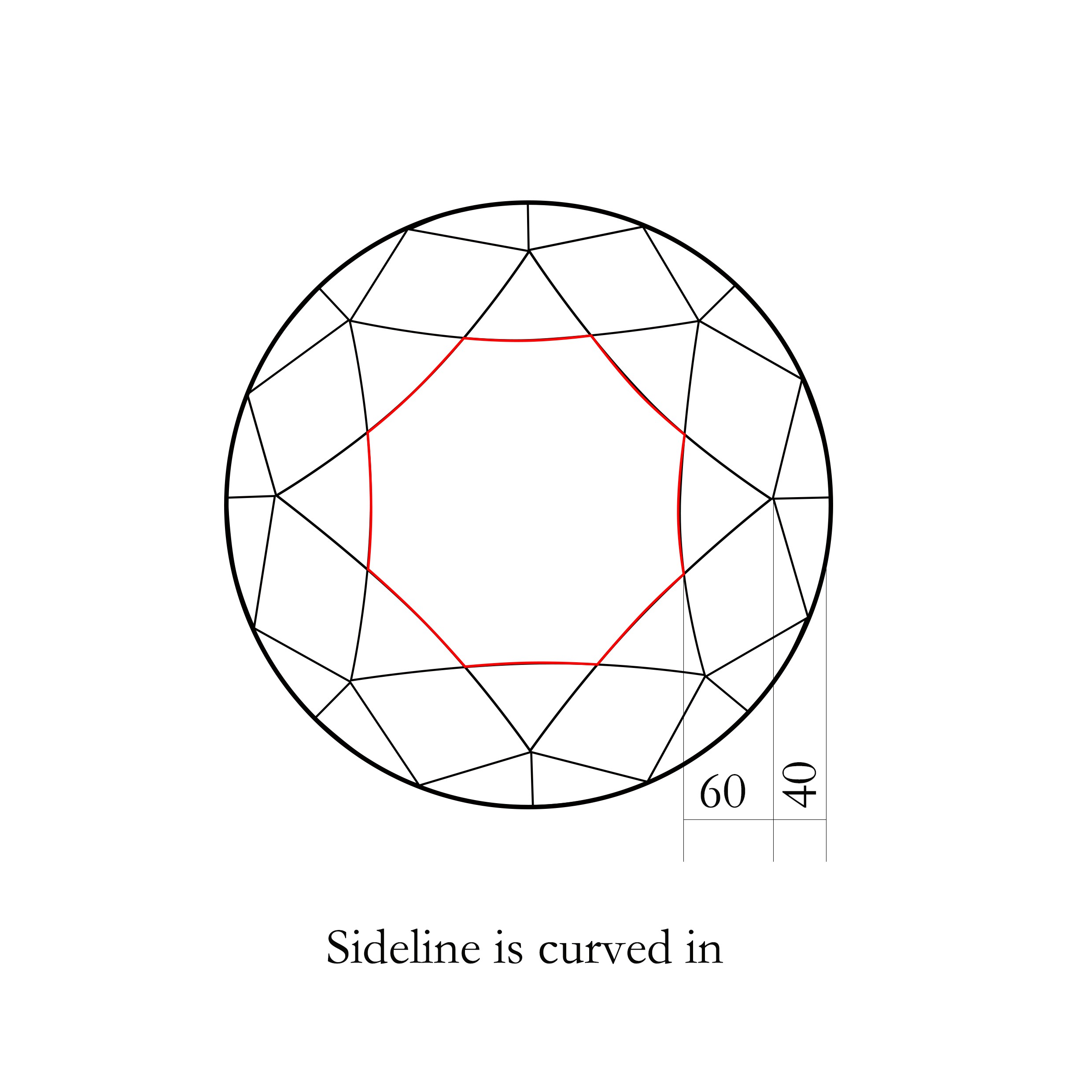
2. Radian method When viewed vertically on the table, the table and the star facets of the round diamond are in the same plane, and it can be seen that the table and the star facets form two overlapping "squares", according to the arc size of the 8 sides of the two "squares" to determine the table width ratio.

When the edge of the "square" is a straight line, the table width ratio is 60%

When the edge of the "square" is slightly curved inward, the table width ratio is about 58% When the edge of the "square" is obviously curved inward, the table width ratio is about 54%
When the sides of the "square" are slightly arched, the table width ratio is about 62% When the edge of the "square" is obviously arched, the table width ratio is about 66%
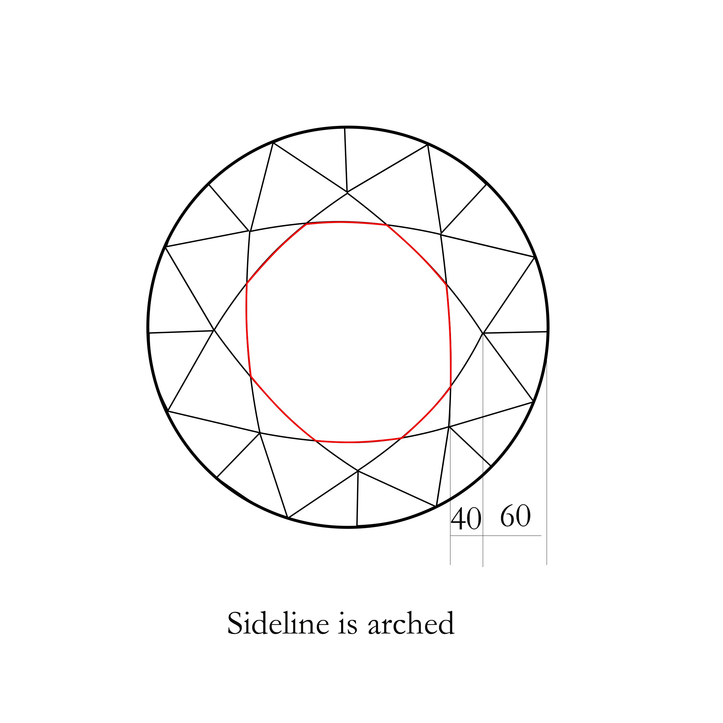
And so on...









Thank you for your liking
YouArticle
已有19人推荐
-

CVD Single-Crystal Diamonds: An Analysis of the Complete Processing Workflow from Gas-Phase Deposition to Finished Diamond Chips
MPCVD (Microwave Plasma Chemical Vapor Deposition) technology is currently the core process for producing high-quality single-crystal diamond s. Thanks to its advantages of low defect rates, high purity, and controllable large dimensions, it is widely used in fields such as semiconductor heat dissipation, precision optics, and high-end sensors. The final quality of single-crystal diamond s depends on comprehensive process control throughout the entire workflow—from vapor deposition growth to pos
-
Single-Crystal or Polycrystalline Diamond — Which Has Greater Potential?
As diamond continues to enter industries such as semiconductors, thermal management, optics, high-power electronics, and precision machining, the requirements for diamond materials are also evolving.
-
Diamond Polishing and Grinding Processes: Core Challenges and Industry Hurdles
Diamond is often hailed as the “ultimate material” – ranking 10 on the Mohs hardness scale, boasting an ultra‑high thermal conductivity (~2,200 W/(m·K)), excellent chemical stability, and broad optical transparency. These properties make it irreplaceable in cutting‑edge applications such as semiconductor heat dissipation, high‑end optics, and quantum chips. Yet the paradox of “good materials are hard to process” is nowhere more evident than in diamond. From rough grinding for planarization to at
-
Single-Crystal vs Polycrystalline CVD Diamond: Process Difference Lies in Growth Logic, Not Equipment
The process difference between single crystal and polycrystalline CVD diamond lies not in equipment, but in growth logic. Single crystal and polycrystalline CVD diamond are two functional new materials with completely independent growth mechanisms, lattice structures and performance systems. Their process logic, product features and application boundaries diverge fundamentally from the very start of deposition and growth. Comparing or selecting materials without considering their underlying crys




