

- 中文
- English
- Español
diamond girdle ratio
2023-05-27 20:22:33
Click:
“
Girdles that are too thin or too thick are not conducive to setting. Too thin girdles cannot withstand impact or pressure, and are prone to damage during setting; diamonds with too thick girdles look smaller than diamonds of the same weight but with slightly thinner girdles. Many, too thick a girdle may leak light, reducing the brilliance of the diamond.
”
The girdle thickness of a polished diamond has relatively little effect on the diamond's brilliance and overall cut aesthetics. Girdles that are too thin or too thick are not conducive to setting. Too thin girdles cannot withstand impact or pressure, and are prone to damage during setting; diamonds with too thick girdles look smaller than diamonds of the same weight but with slightly thinner girdles. Many, too thick a girdle may leak light, reducing the brilliance of the diamond. Therefore, a well-cut diamond should have a moderate girdle thickness.
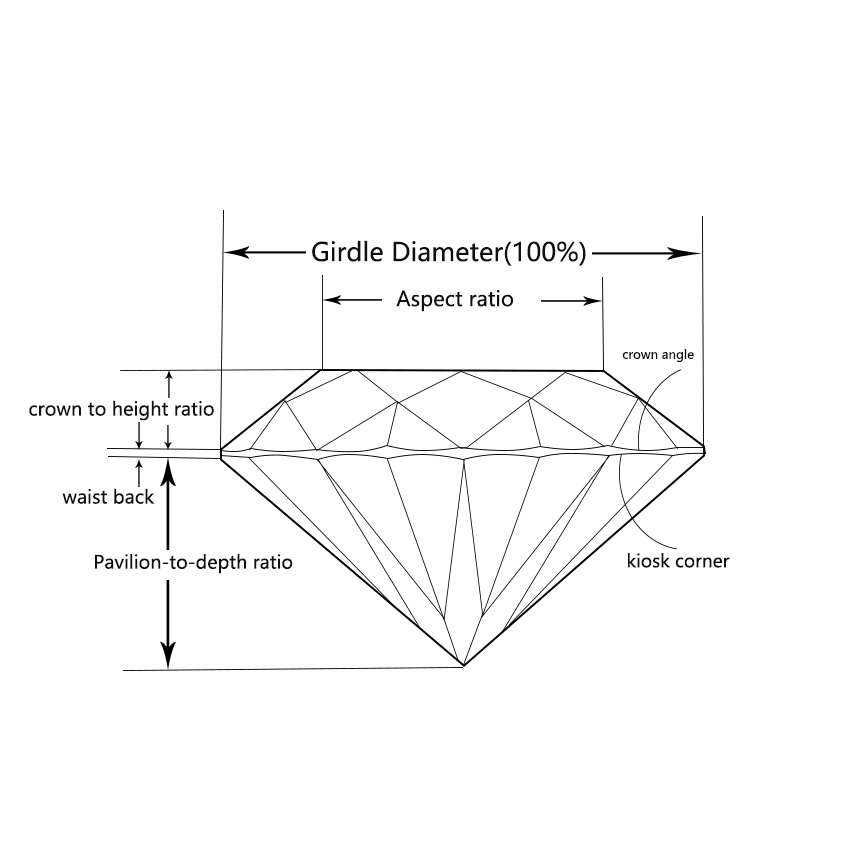
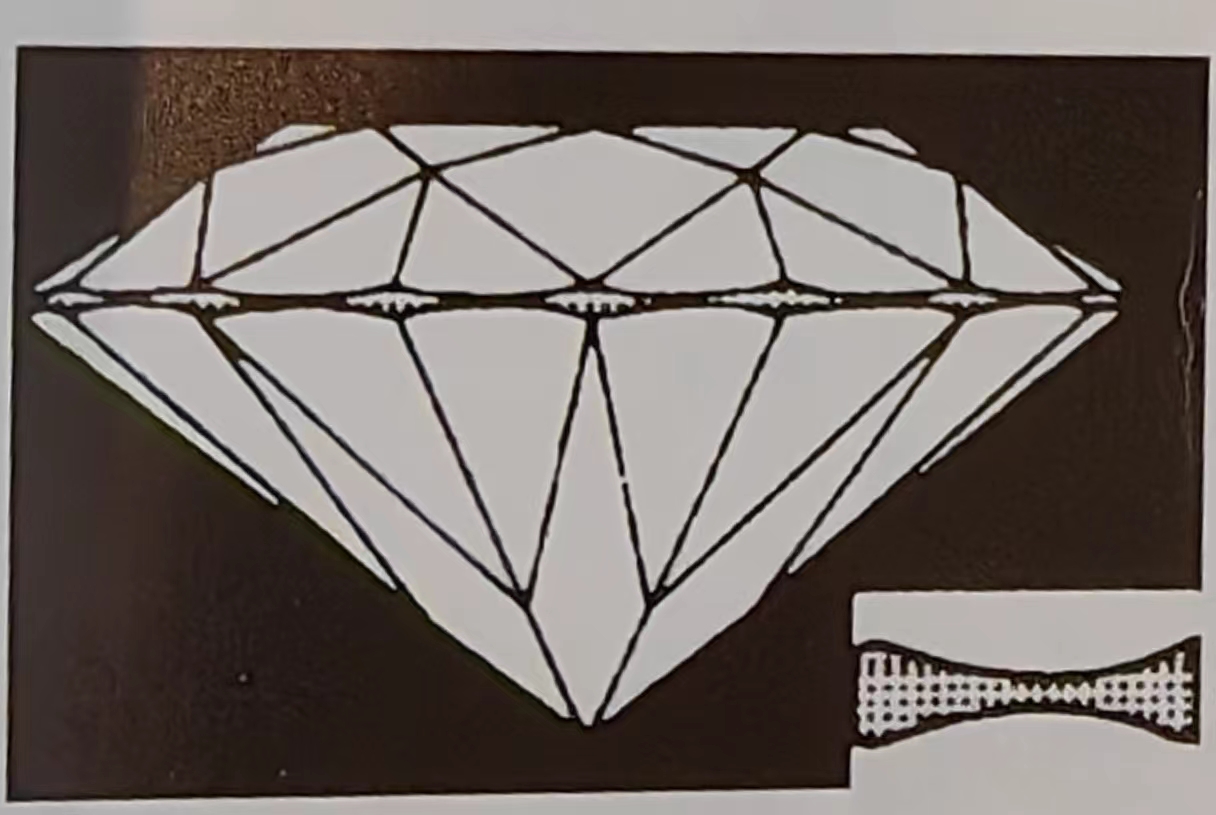
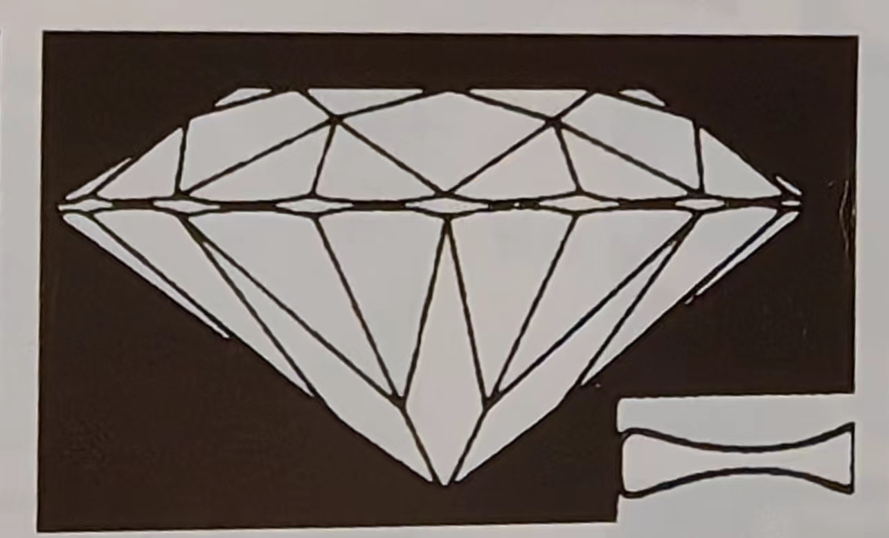
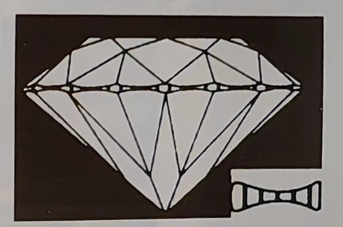
Polished girdles, polished girdles, and faceted girdles come in three types of polished girdles.
Polishing the girdle is processed by a car drilling machine. The surface of the girdle is rough and dull, usually off-white and opaque. This is the most common shape of the girdle;
Polishing the girdle is processed on a diamond micropowder grinding wheel with a smoothing machine. The surface of the girdle is translucent and smooth, and it is often used as a repairing behavior for diamonds with symmetry defects;
The faceted girdle is processed by hand with a grinding machine. The girdle presents multiple facets, which are smooth and translucent, but the size of the facets usually varies, which is often due to the fact that the diamond girdle is too thick or the girdle is flawed. The repair method for it.
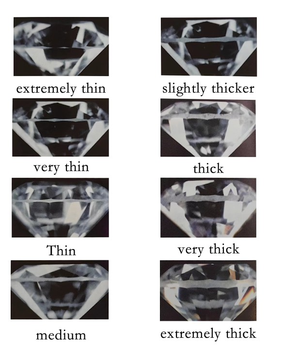
When visually evaluating, the side of the diamond is clamped, or the table and bottom facets are oppositely clamped, the line of sight is parallel to the girdle plane, the girdle is observed for a week with a 10 times magnifying glass and the naked eye, and the main thickness of the entire girdle is taken as the girdle of the diamond. Girdle thickness, the girdle thickness is divided into seven levels: very thin, very thin, thin, medium, thick, very thick and extremely thick.
(1) Extremely thin (knife-edge) with an actual thickness of less than 0.035mm, which is blade-like under a 10x magnifying glass and invisible to the naked eye.
(2) Very thin The actual thickness is less than 0.10mm, and it appears as a thin line under a 10x magnifying glass, which is almost invisible to the naked eye.
(3) The actual thickness is less than 0.20mm, and the width is narrow under a 10x magnifying glass, which is difficult to see with the naked eye.
(4) The medium actual thickness is less than 0.30mm, with a clear width under a 10x magnifying glass, and a thin line when observed with the naked eye.
(5) Thickness The actual thickness is less than 0.50mm, and the width is obvious under a 10x magnifying glass, and the width is narrow when observed with the naked eye.
(6) Very thick, the actual thickness is less than 0.75mm, the width is unsightly under a 10x magnifying glass, and the naked eye observation is clear width.
(7) Extremely thick The actual thickness is greater than 0.80mm, and the width is very unsightly under a 10x magnifying glass, and the width is obvious when observed with the naked eye.









Prev : How to Visually Measure the Depth Ratio of a Diamond Pavilion
Next : Have you noticed the size of the culet of the loose diamond?
Thank you for your liking.
YouArticle
已有26人推荐
-

Foshan Highlight Intelligent Technology invites you to the 140th Canton Fair—join us at Booth 21.2A23-24 in the Friendship Hall to share in the brilliance.
Foshan Highlight Intelligent Technology invites you to the 140th Canton Fair—join us at Booth 21.2A23-24 in the Friendship Hall to share in the brilliance.
-
CVD Single-Crystal Diamonds: An Analysis of the Complete Processing Workflow from Gas-Phase Deposition to Finished Diamond Chips
MPCVD (Microwave Plasma Chemical Vapor Deposition) technology is currently the core process for producing high-quality single-crystal diamond s. Thanks to its advantages of low defect rates, high purity, and controllable large dimensions, it is widely used in fields such as semiconductor heat dissipation, precision optics, and high-end sensors. The final quality of single-crystal diamond s depends on comprehensive process control throughout the entire workflow—from vapor deposition growth to pos
-
Single-Crystal or Polycrystalline Diamond — Which Has Greater Potential?
As diamond continues to enter industries such as semiconductors, thermal management, optics, high-power electronics, and precision machining, the requirements for diamond materials are also evolving.
-
Diamond Polishing and Grinding Processes: Core Challenges and Industry Hurdles
Diamond is often hailed as the “ultimate material” – ranking 10 on the Mohs hardness scale, boasting an ultra‑high thermal conductivity (~2,200 W/(m·K)), excellent chemical stability, and broad optical transparency. These properties make it irreplaceable in cutting‑edge applications such as semiconductor heat dissipation, high‑end optics, and quantum chips. Yet the paradox of “good materials are hard to process” is nowhere more evident than in diamond. From rough grinding for planarization to at




