

- 中文
- English
- Español
Have you noticed the size of the culet of the loose diamond?
2023-06-01 20:22:33
Click:
“
However, if the bottom facet is too large, all the light incident on the bottom facet from the front will leak out of the diamond, and it will appear as a small dark window when viewed from the front, which will have a negative impact on the appearance. The purpose of cutting the bottom facet is to protect the tip of the pavilion.
”
The culet is the smallest facet of all the facets in a diamond and has less effect on the diamond's brilliance. However, if the bottom facet is too large, all the light incident on the bottom facet from the front will leak out of the diamond, and it will appear as a small dark window when viewed from the front, which will have a negative impact on the appearance. The purpose of cutting the bottom facet is to protect the tip of the pavilion.
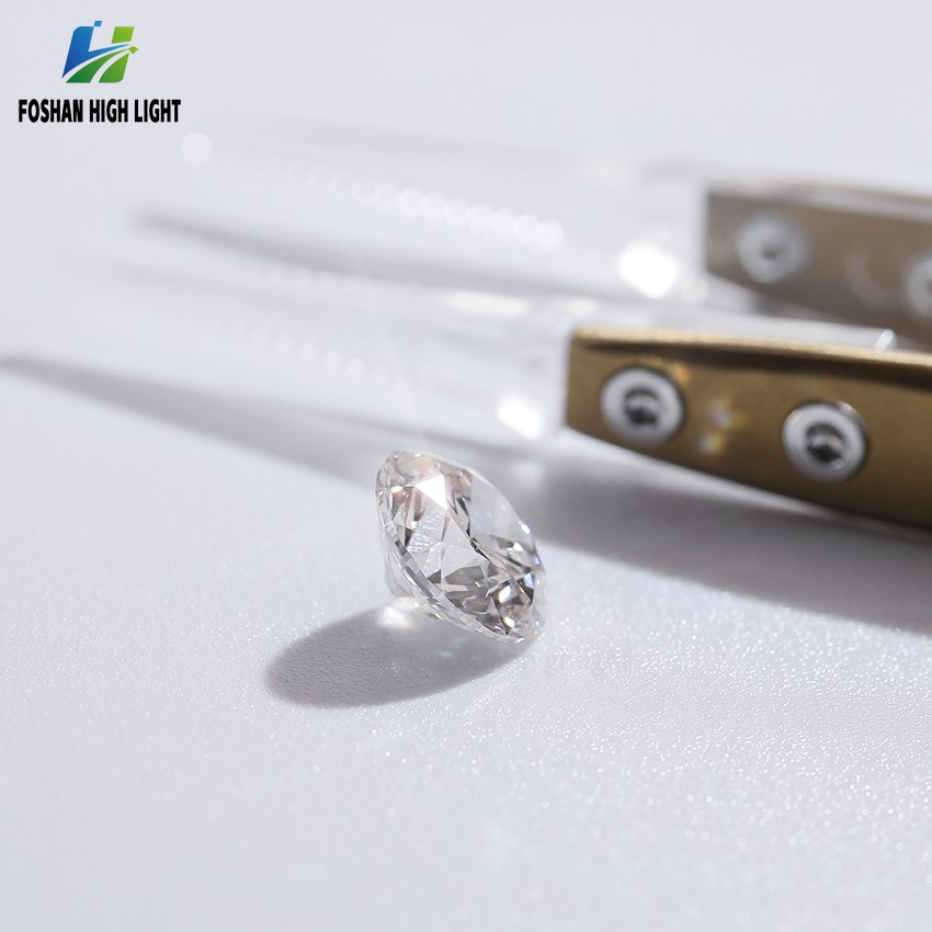
The modern method of cutting diamonds is to not cut the culet but to leave a point culet. The dotted culet is easily damaged, forming a small white break, which is also very bad for the diamond. Therefore, it is reasonable to reserve a bottom facet of a suitable size. The bottom facet must achieve the purpose of not affecting the appearance and protecting the tip of the pavilion. This bottom facet should be invisible or difficult to see with the naked eye.
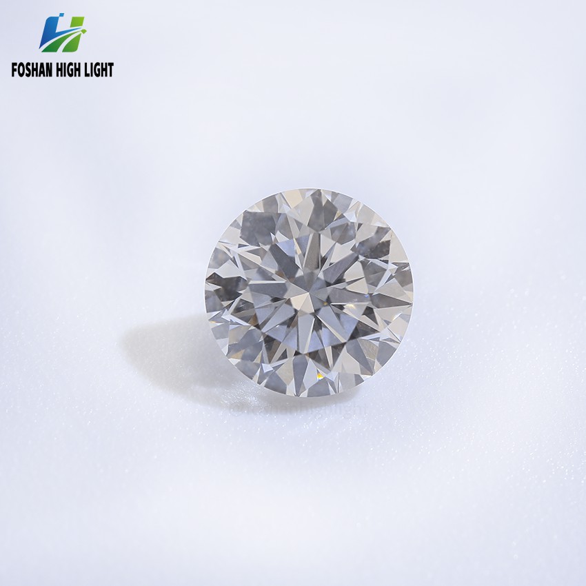
When visually evaluating, the table top faces upwards, the line of sight is vertical to the table top, and the bottom surface can be divided into the following six grades according to the size.
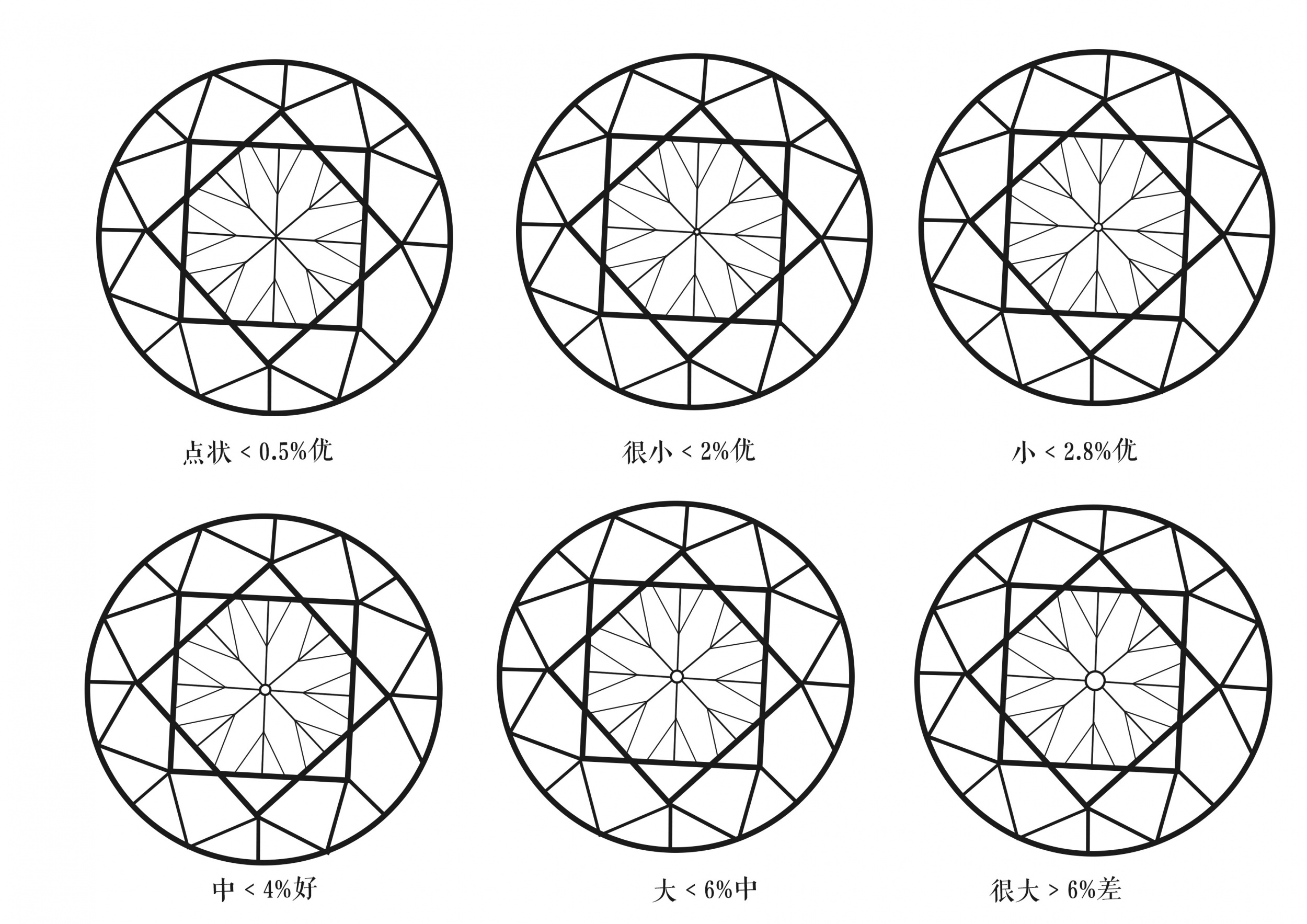
(1) Spot shape: the absolute diameter is less than 0.04mm, and it appears as small white spots under a 10x magnifying glass, which is invisible to the naked eye.
(2) Very small: the absolute diameter is less than 0.12mm, the outline is difficult to distinguish under a 10x magnifying glass, and it is invisible to the naked eye.
(3) Small: The absolute diameter is within 0.13~0.18mm, and the octagonal outline can be seen under a 10x magnifying glass, but invisible to the naked eye.
(4) Medium: The absolute diameter is within 0.19~0.24mm, and the octagonal facets can be seen under a 10x magnifying glass, which can be seen with the naked eye.
(5) Large: The absolute diameter ranges from 0.25 to 0.38mm, and the small surface of the bottom is obvious under a 10x magnifying glass, and an octagon can be seen with the naked eye.
(6) Very large: the absolute diameter is greater than 0.38mm, the bottom surface is obvious under a 10x magnifying glass, and the octagon is easy to see with the naked eye.









-

CVD Single-Crystal Diamonds: An Analysis of the Complete Processing Workflow from Gas-Phase Deposition to Finished Diamond Chips
MPCVD (Microwave Plasma Chemical Vapor Deposition) technology is currently the core process for producing high-quality single-crystal diamond s. Thanks to its advantages of low defect rates, high purity, and controllable large dimensions, it is widely used in fields such as semiconductor heat dissipation, precision optics, and high-end sensors. The final quality of single-crystal diamond s depends on comprehensive process control throughout the entire workflow—from vapor deposition growth to pos
-
Single-Crystal or Polycrystalline Diamond — Which Has Greater Potential?
As diamond continues to enter industries such as semiconductors, thermal management, optics, high-power electronics, and precision machining, the requirements for diamond materials are also evolving.
-
Diamond Polishing and Grinding Processes: Core Challenges and Industry Hurdles
Diamond is often hailed as the “ultimate material” – ranking 10 on the Mohs hardness scale, boasting an ultra‑high thermal conductivity (~2,200 W/(m·K)), excellent chemical stability, and broad optical transparency. These properties make it irreplaceable in cutting‑edge applications such as semiconductor heat dissipation, high‑end optics, and quantum chips. Yet the paradox of “good materials are hard to process” is nowhere more evident than in diamond. From rough grinding for planarization to at
-
Single-Crystal vs Polycrystalline CVD Diamond: Process Difference Lies in Growth Logic, Not Equipment
The process difference between single crystal and polycrystalline CVD diamond lies not in equipment, but in growth logic. Single crystal and polycrystalline CVD diamond are two functional new materials with completely independent growth mechanisms, lattice structures and performance systems. Their process logic, product features and application boundaries diverge fundamentally from the very start of deposition and growth. Comparing or selecting materials without considering their underlying crys




