

- 中文
- English
- Español
Huawei and Harbin Institute of Technology jointly publish patents for three-dimensional integrated chips based on silicon and diamond
2023-12-01 11:19:44
Click:
“
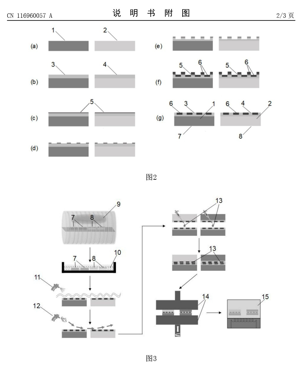
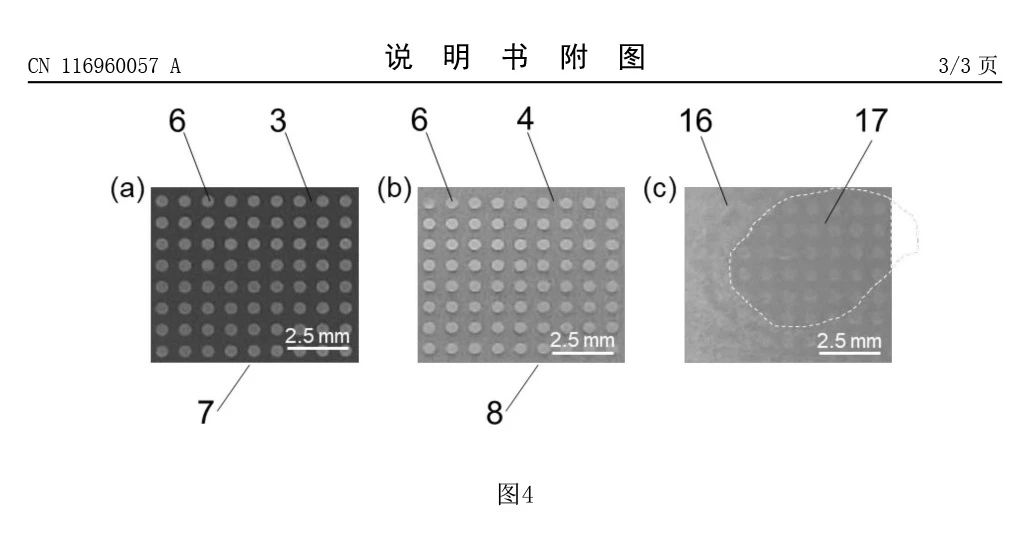
Recently, a patent for "a hybrid bonding method for three-dimensional integrated chips based on silicon and diamond" applied by Huawei Technologies Co., Ltd. and Harbin Institute of Technology was published. The substantive review will take effect on November 14. This invention patent will greatly benefit diamond
”
Recently, a patent for "a hybrid bonding method for three-dimensional integrated chips based on silicon and diamond" applied by Huawei Technologies Co., Ltd. and Harbin Institute of Technology was published. The substantive review will take effect on November 14. This invention patent will greatly benefit the development of the diamond industry, provide important basis and reference for the application of diamond chips, and promote major changes in the field of chip manufacturing.
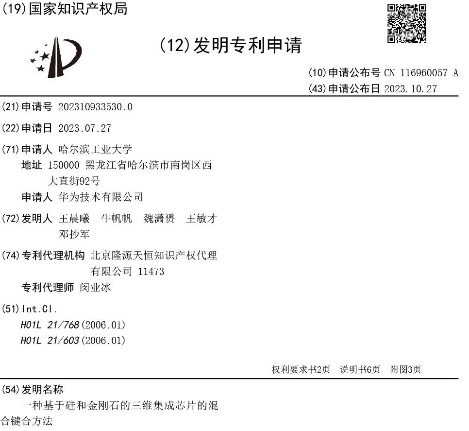
It is understood that the mainstream direction of the development of the semiconductor industry is three-dimensional integration technology. However, as the integration density continues to increase and feature sizes continue to shrink, the thermal management of electronic chips faces great challenges. The heat accumulated inside the chip is difficult to transfer to the heat sink on the package surface, resulting in a sudden increase in internal junction temperature, which seriously threatens chip performance, stability, and service life.
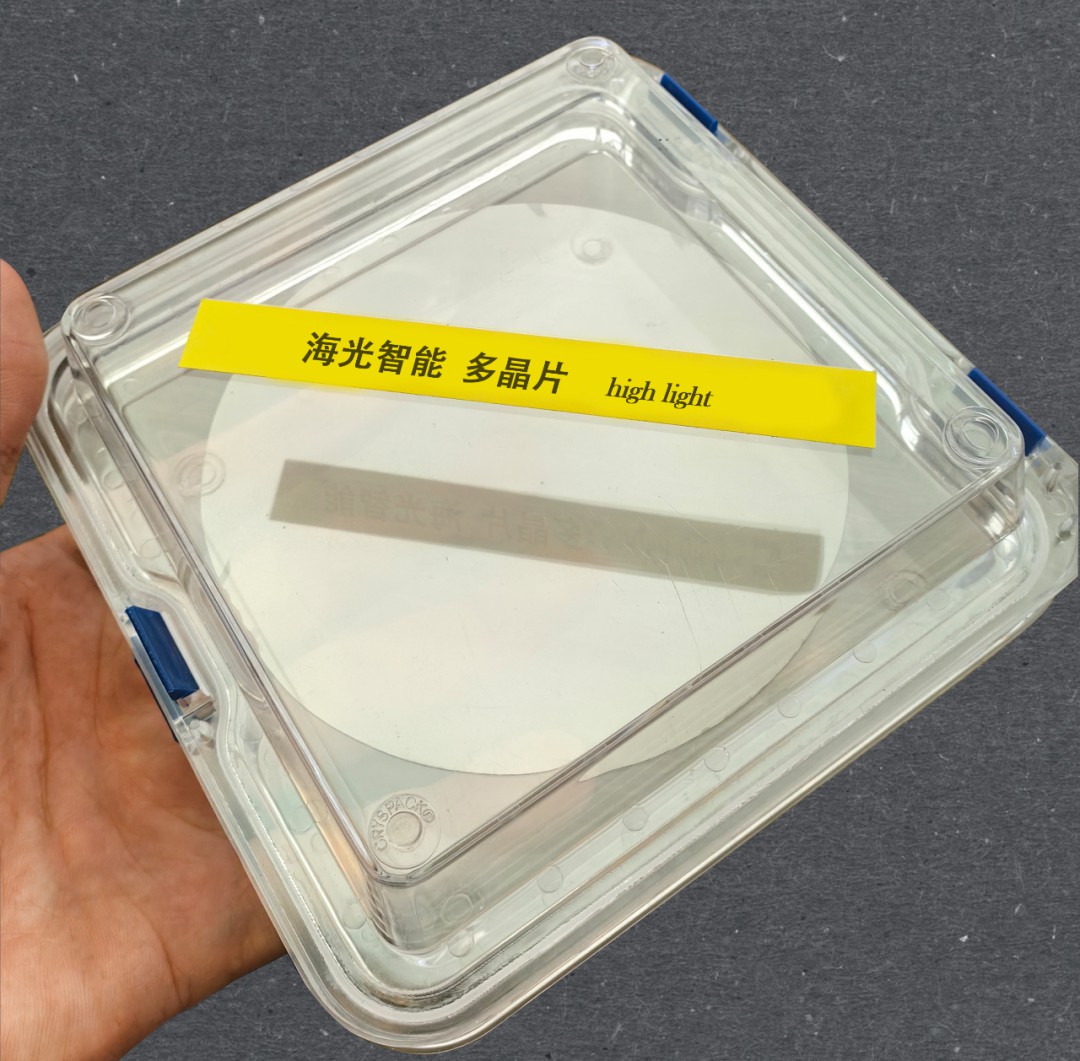
As a semiconductor diamond production supplier, High Light Intelligence Technology is developing rapidly in the semiconductor industry. We also provide diamond materials to major commercial customers and academic researchers, contributing to the development of semiconductor technology and materials.


-

Z-Axis System: The Key to Stable Production of MPCVD Diamonds
Microwave Plasma Chemical Vapor Deposition is the mainstream method for producing high-quality diamonds in the industry. When the equipment is running, it first pumps the reaction chamber into a vacuum state to strictly ensure the chamber is fully sealed and airtight. Then, the microwave device releases energy, and special mixed reaction gases are fed into the chamber. Under the action of energy, a stable plasma area is formed. These highly active plasmas provide stable heat and reaction conditi
-
How to Choose the Right MPCVD Equipment?
MPCVD equipment is a critical asset across a wide range of industries, including industrial manufacturing, semiconductor thermal management, precision cutting tools, and lab-grown diamonds. Choosing the right equipment not only boosts production efficiency and ensures consistent product quality but also effectively controls long-term costs, making your entire production process smoother and more competitive. Many people struggle with the question: How do I make the right choice? Today, drawing o
-
CVD Diamond Clarity: How to Avoid Inclusions That Affect Jewelry Value
After selecting a loose diamond, the setting not only determines the diamond’s security but also directly affects its perceived size. With diamonds of the same weight, choosing the right setting design can effortlessly create the surprise of “small carats making a big impact,” saving on your budget while enhancing the diamond’s quality. Among these, pavé and prong settings are the two most classic and effective ways to make a diamond appear larger. Paired with specialized designs that maximize t
-
How Diamond Became the Ultimate Thermal Solution in the Era of Computing Power
The iconic narrative behind the legendary "A Diamond is Forever" slogan has long been upended by China's industrial prowess. Once synonymous with luxury and rarity, this gem has shed its glamorous aura to become an indispensable thermal management material for high-power devices. In an era of explosive growth in AI computing power, it has taken up the mantle of "cooling to save computing power".


