- 中文
- English
- Español
Advantages of High Light Intelligence Technology’s single crystal and polycrystalline products
2024-01-24 09:07:48
Click:
“
With the continuous development of science and technology, the semiconductor industry is also rising rapidly. In this field, diamond single crystal and polycrystalline products are one of the mainstream choices on the market. As a semiconductor diamond production supplier, High Light Intelligence Technology's single crystal and polycrystalline products have significant advantages in the market.
”
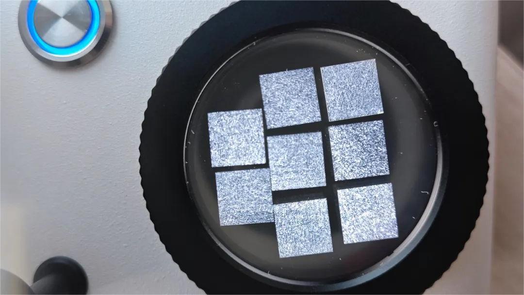
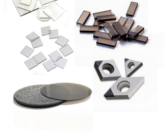
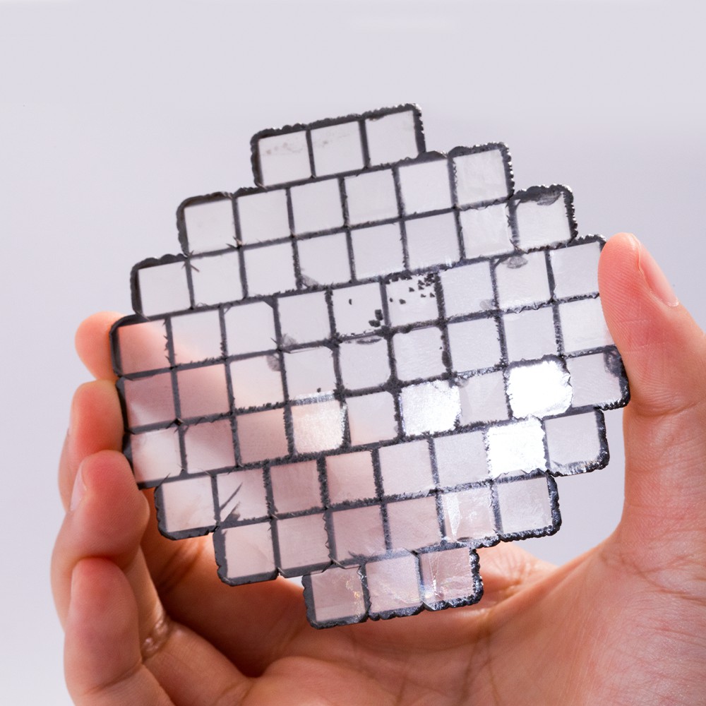
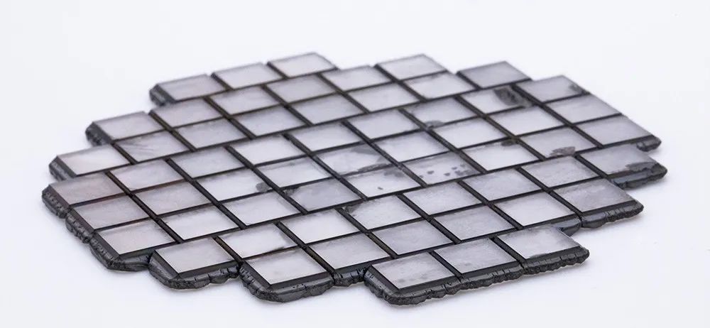
In the fields of materials science and engineering, diamond single crystals have attracted much attention due to their unique physical and chemical properties. Depending on the application area, there are significant differences in manufacturing, purity, appearance, and purpose of use between industrial single crystal and jewelry single crystal. At present, High Light Intelligence Technology's single crystal products have high transmittance, high thermal conductivity, low surface roughness after polishing, no impurities when inspected under a 50x magnifying glass, no cracks on the edges, and uniform stress distribution. They can be professionally customized according to customer requirements.
Manufacturing technology:
Industrial single crystals are mainly grown using MPCVD (microwave plasma chemical vapor deposition) technology. This method can prepare high-purity, high-quality diamond films over a large area, so it is widely used in industrial fields.
Purity and performance:
The purity requirement of industrial single crystal is generally above 90% to ensure its high hardness, high thermal conductivity, low thermal expansion coefficient and other characteristics. These properties make industrial single crystal an ideal material for manufacturing cutting tools, abrasives, electronic devices and other products.
Stability and reliability:
Industrial single crystal has a basically complete crystal structure, so it has good stability and reliability during long-term use. This characteristic makes it widely used in solar power stations, large-scale photovoltaic projects and other fields. And due to the regularity and stability of its crystal structure, industrial single crystals have high photoelectric conversion efficiency and long service life. This gives it a high return on investment in photovoltaic projects.
Application areas:
Due to its excellent physical properties, industrial single crystals are widely used in manufacturing tools, cutting tools, abrasives, automobile manufacturing, aerospace, precision machinery and other fields. They have excellent wear resistance and service life during cutting, grinding, polishing and other processing processes. And due to the integrity of its crystal structure, industrial single crystal has good electrical conductivity and mechanical strength. Industrial single crystal can also be used in semiconductor devices, integrated circuits, electronic components and other fields.
Manufacturing technology:
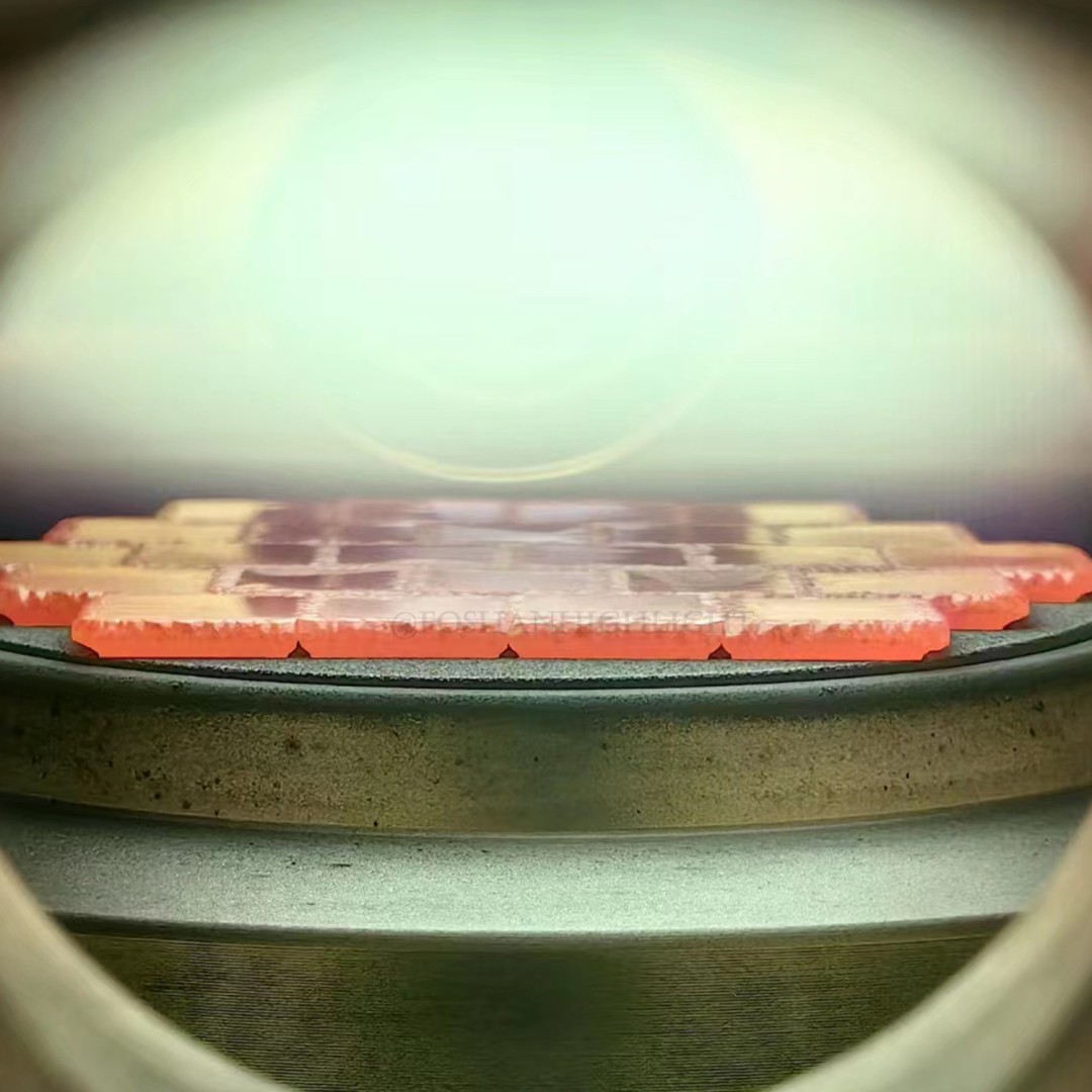
Jewelry single crystals are usually grown using MPCVD (microwave plasma chemical vapor deposition) technology. This method can produce high-purity, high-optical-quality diamond crystals.
Purity and appearance:
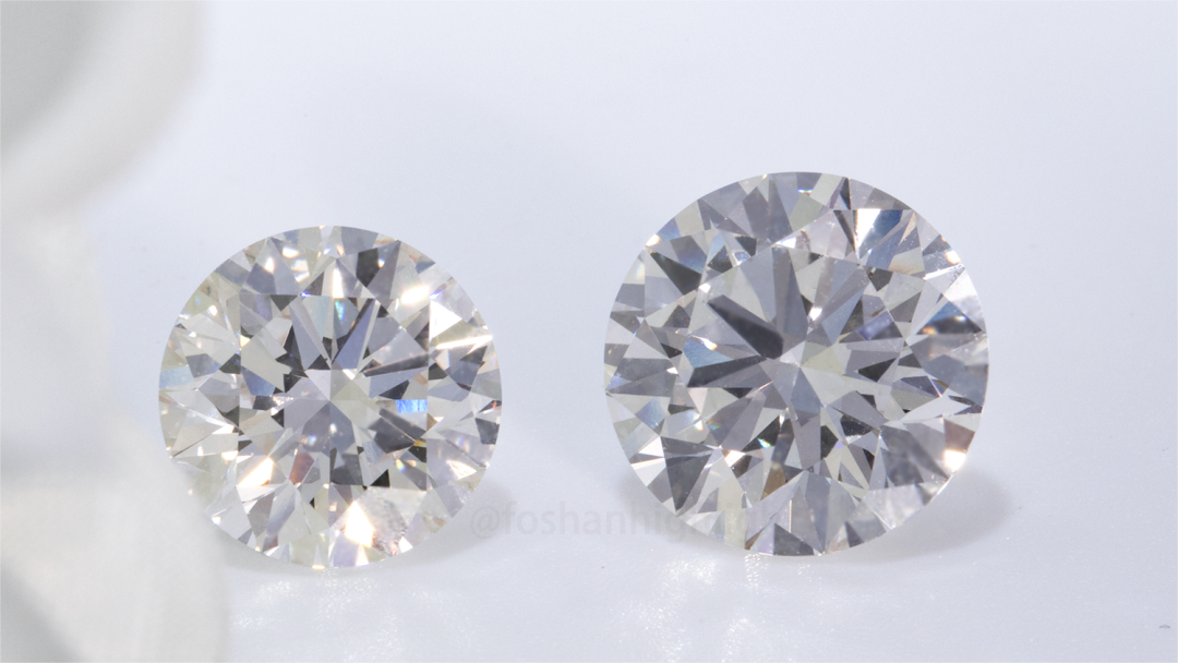
The purity of jewelry single crystal is as high as 99.99% or more, with a dazzling appearance and extremely high gloss and refractive index. They are usually colorless and transparent in color and have a very uniform internal structure, making their appearance more beautiful. It can be used to make jewelry, high-end decorations, etc.
Application areas:
In addition to traditional jewelry and decoration fields, jewelry single crystal is also used in high-end watch manufacturing, optical instruments and precision instrument manufacturing and other fields. They excel in these areas due to their high hardness and wear resistance.
Crystal Structure:
Whether it is industrial or jewelry single crystal, they have a complete crystal structure, which makes them consistent in certain physical and chemical properties.
Hardness and wear resistance:
Since diamond is the hardest substance known in nature, whether it is industrial or jewelry single crystal, it has extremely high hardness and wear resistance.
Market prospects:
With the continuous advancement of science and technology and the development of various industries, the application fields of single crystal products continue to expand. The demand for industrial in the manufacturing industry single crystals continues to grow, while jewelry single crystals is also highly sought after in the high-end market.
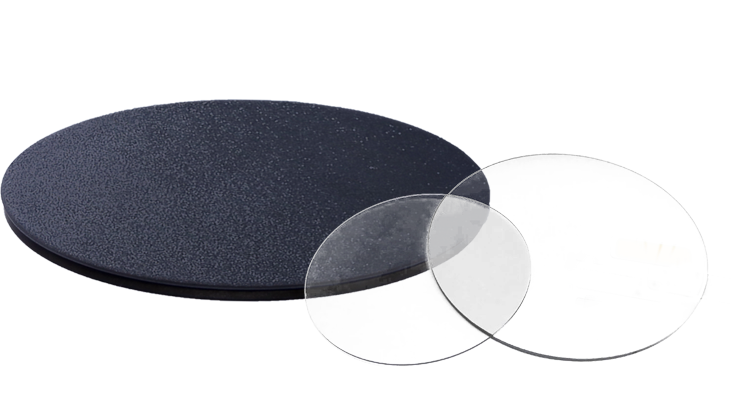
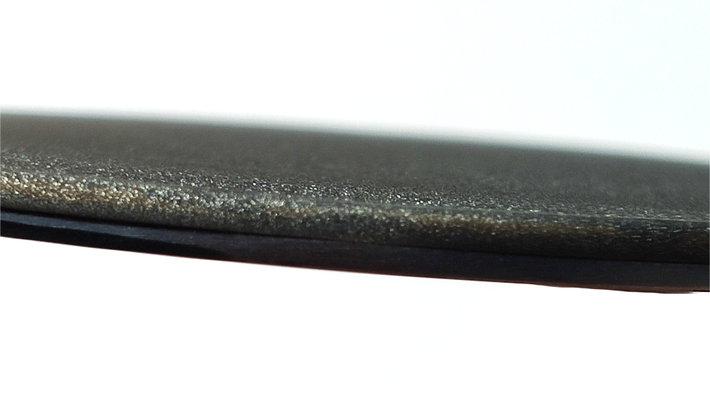
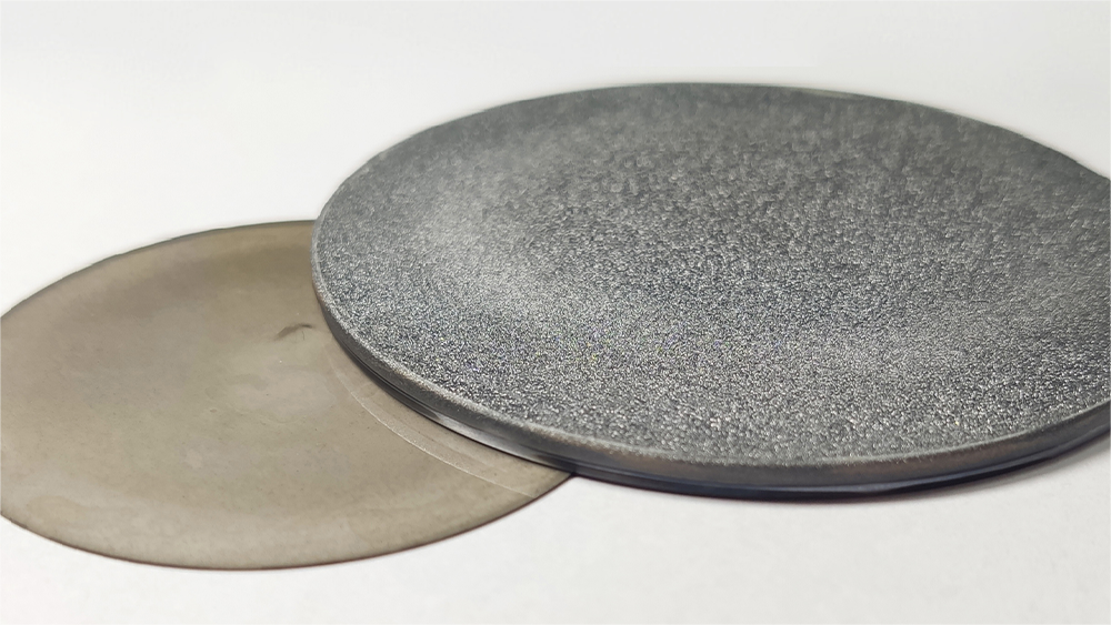
High Light Intelligence Technology's polycrystalline products have smooth surfaces and low warpage, adapting to various installation environments. The product diameter can reach 100mm, and they have higher efficiency and economy in the production process.
Hardness and wear resistance:
Our polycrystalline products have extremely high hardness and very good wear resistance. They have excellent durability and service life during cutting, grinding, polishing and other processing processes, and can ensure the quality and accuracy of the processed surface. .
High thermal conductivity:
It has extremely high thermal conductivity and can quickly conduct heat and reduce temperature, thereby reducing thermal damage and improving processing efficiency.
Chemical stability:
It shows good chemical stability in high temperature, high pressure and highly corrosive environments, is not easily oxidized or corroded, and can maintain stable performance.
High optical quality:
With the characteristics of high transparency and low dispersion, it can produce high-quality optical components and lasers, which are widely used in fields such as optics, optoelectronics and laser technology.
Environmental protection and sustainability:
The growth process of polycrystalline is relatively environmentally friendly, and its long service life reduces the possibility of frequent replacement and abandonment, which meets the requirements of sustainable development.
Economic benefits:
Compared with traditional processing materials, our polycrystalline products have higher processing efficiency and longer service life. Their excellent performance and long service life make the overall economic benefits relatively high, and can provide Businesses save a lot of costs.
Whether it is single crystal or polycrystalline products, Haiguang Intelligent Technology shows excellent performance and quality. Customers can choose products that suit them according to their own needs. High Light Intelligence Technology, as a semiconductor diamond production supplier, while the semiconductor industry is developing rapidly, we also provide diamond materials to major commercial customers and academic researchers, contributing to the development of semiconductor technology and materials. With MPCVD technology as the core, we have long been committed to the R&D and manufacturing of high-quality diamond materials and related equipment. We have advanced MPCVD equipment, laser processing equipment and precision polishing equipment.









-

Single-Crystal vs Polycrystalline CVD Diamond: Process Difference Lies in Growth Logic, Not Equipment
The process difference between single crystal and polycrystalline CVD diamond lies not in equipment, but in growth logic. Single crystal and polycrystalline CVD diamond are two functional new materials with completely independent growth mechanisms, lattice structures and performance systems. Their process logic, product features and application boundaries diverge fundamentally from the very start of deposition and growth. Comparing or selecting materials without considering their underlying crys
-
From Lab-Grown Diamonds to Industrial Diamonds: Is It Time to Build an MPCVD Factory?
The lab-grown diamond industry is entering a new stage. Over the these few years, lab-grown diamonds have gradually gained wider acceptance in the jewelry market. With the development of production technology, equipment maturity and supply chain improvement, the industry is becoming more standardized and efficient. But beyond jewelry, another opportunity is attracting more attention:Industrial diamond applications.
-
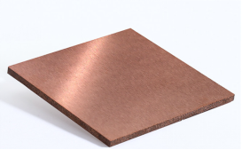
Diamond‑Copper Composite: A Next‑Generation Solution for High‑Power Electronics Thermal Management
Diamond‑copper composite (DC) is an advanced metal‑matrix composite material consisting of diamond particles as the reinforcement phase and copper as the matrix, fabricated through state‑of‑the‑art composite preparation techniques. Diamond has the highest thermal conductivity of any naturally occurring material, with isotropic values ranging from 1200 to 2300 W/m·K. Copper, with a thermal conductivity of 401 W/m·K, ranks second only to silver among common metals. By combining the two, the compo
-
Mosaic Single‑Crystal Diamond: Breaking Size Limits
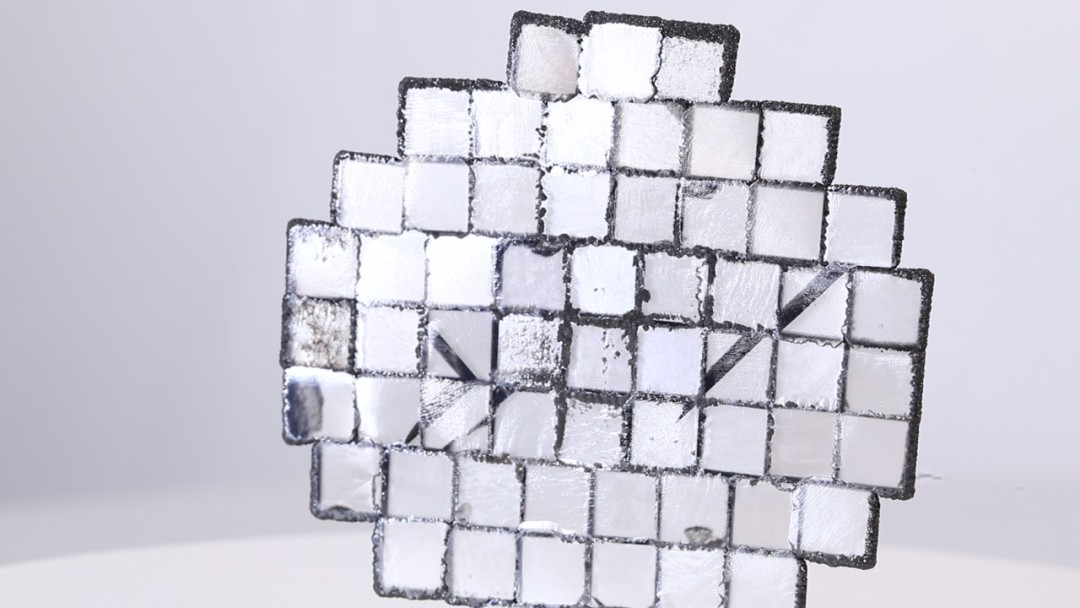
With an ultra‑wide bandgap of 5.47 eV, ultra‑high thermal conductivity (>2000 W/m·K), high carrier mobility (electron mobility up to 4500 cm²·V⁻¹·s⁻¹), and ultra‑high theoretical breakdown field strength (>10 MV/cm), Single‑Crystal Diamond (SCD) is an ideal candidate for next‑generation high‑power, high‑frequency and extreme‑environment electronic devices. However, both natural diamond and HPHT‑synthesized single‑crystal diamond are limited in lateral size, which greatly hinders large‑scal