- 中文
- English
- Español
Diamond heat sink boosts heat dissipation in advanced packaging
2024-09-11 09:29:05
Click:
“
Cutting-edge technologies such as AI and cloud computing are making great strides with the help of high-performance chips, and with global and Chinese technology companies jointly promoting development, smart hardware chips will usher in explosive growth.
”
AI, deep learning, cloud computing, supercomputing and other cutting-edge technologies drive technological leaps, with high-performance chips as the common foundation. Global technology giants such as Google, Amazon, Intel, Nvidia, and AMD are deeply engaged in this field; Chinese companies such as Huawei, Alibaba, Baidu, and Tencent are also actively contributing to the AI wave. In the future, intelligent hardware chips such as CPU, GPU, ASIC, and FPGA will usher in explosive growth.

Moore's Law Slows Down

What is 2.5D packaging?
TrendForce reports that the surge in generative AI applications such as chatbots has prompted a significant expansion of AI server development in 2023 and is highly dependent on high-end chips. It is expected to drive a 30% to 40% increase in advanced packaging production capacity in 2024. Advanced packaging is located at the intersection of wafer manufacturing and packaging and testing, involving IDM, foundry and packaging and testing companies, and the market is highly concentrated. The world's six largest manufacturers account for more than 80% of the market share, including Intel, Samsung (IDM), TSMC (OEM), and ASE, Amkor, and JCET (the top three in packaging and testing).

Yole's report predicts that the advanced packaging market will reach $37.5 billion in 2021, accounting for 44% of the total, and is expected to increase to 53% in 2027, or about $65 billion. Among them, 2.5D/3D packaging is widely used in (x)PU, ASIC, FPGA, 3D NAND, HBM, CIS, etc. 2.5D packaging technology has emerged since the 2010s, providing solutions for high-density integration of heterogeneous chips. It adopts a three-layer three-dimensional structure: chip micro-bump flip-chip, TSV dielectric layer connecting the upper and lower layers, and dielectric layer flip-chip to the substrate. This complex structure aims to shorten the distance between chips, improve computing speed, signal quality and reduce energy consumption, and promote packaging technology into the 2.5D era.
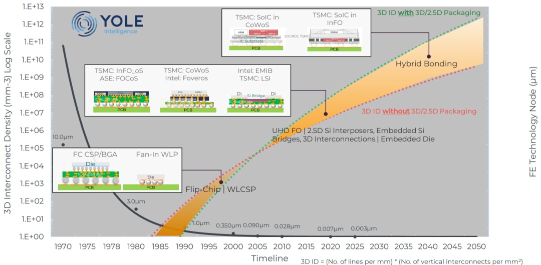
HBM requires high connection density, which cannot be met by traditional FCBGA, so 2.5D silicon dielectric layer technology is used. SoC designs are diverse, and some use 2.5D packaging to integrate SerDes and the main chip. High-end chips tend to be multi-chiplet designs, and 2.5D packaging is used to improve yield and reduce costs. TSV technology in 2.5D achieves high-density connection, which is completed by OSAT factories. Amkor leads 2.5D packaging and launches CoS and CoW platforms, which have been mass-produced since 2014 and 2018 respectively. CoS first attaches the dielectric layer and then the chip, and uses RDL First to improve yield.

CoW packaging is an upgrade of CoS, using silicon wafers as substrates. The chip is first attached to the dielectric layer, then wafer-level plastic sealing is performed, and finally the substrate is connected. Its advantage lies in the enhanced physical structure, which is suitable for large chip and dielectric layer packaging. As a TSV-free CoW variant, HDFO achieves high-density connection and low cost. It is a new trend in heterogeneous packaging and has been applied to network communications, servers, and GPU/FPGA. TSMC's CoWoS technology combines CoW and oS to improve performance, reduce power consumption and reduce size, consolidating its leadership in packaging technology. CoWoS key technologies include multi-chip integration, high-density silicon dielectric layer interconnection and efficient heat dissipation.

CoS/CoWoS Cooling Solution
CoWoS packaging dissipates heat efficiently, maintains high-performance computing stability, and optimizes heat dissipation through multi-layer heat sinks, TSV, and complex thermal management structures. Its non-gel TIM improves thermal conductivity and reliability. At high integration, CoWoS has high cost but excellent heat dissipation. CoS simplifies packaging and has low thermal resistance, but heat dissipation is limited at high power, requiring additional heat dissipation measures. Diamond heat sink materials have become a new favorite in thermal management due to their excellent thermal conductivity and other characteristics.

Diamond Heat Sink Cooling Solution
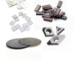
At present, semiconductor materials such as Si, SiC, and GaN have limited thermal conductivity and cannot meet the heat dissipation needs of high-power electronic devices. Diamond has become the focus of future heat dissipation solutions with its ultra-high thermal conductivity, and both single crystal and polycrystalline are superior to traditional materials. The direct connection technology between diamond and semiconductor is the key, which directly affects the heat dissipation effect. The main methods include deposition process and low-temperature bonding technology.











-

Single-Crystal vs Polycrystalline CVD Diamond: Process Difference Lies in Growth Logic, Not Equipment
The process difference between single crystal and polycrystalline CVD diamond lies not in equipment, but in growth logic. Single crystal and polycrystalline CVD diamond are two functional new materials with completely independent growth mechanisms, lattice structures and performance systems. Their process logic, product features and application boundaries diverge fundamentally from the very start of deposition and growth. Comparing or selecting materials without considering their underlying crys
-
From Lab-Grown Diamonds to Industrial Diamonds: Is It Time to Build an MPCVD Factory?
The lab-grown diamond industry is entering a new stage. Over the these few years, lab-grown diamonds have gradually gained wider acceptance in the jewelry market. With the development of production technology, equipment maturity and supply chain improvement, the industry is becoming more standardized and efficient. But beyond jewelry, another opportunity is attracting more attention:Industrial diamond applications.
-
Diamond‑Copper Composite: A Next‑Generation Solution for High‑Power Electronics Thermal Management
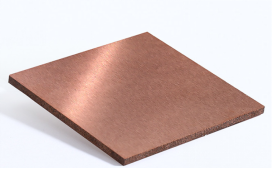
Diamond‑copper composite (DC) is an advanced metal‑matrix composite material consisting of diamond particles as the reinforcement phase and copper as the matrix, fabricated through state‑of‑the‑art composite preparation techniques. Diamond has the highest thermal conductivity of any naturally occurring material, with isotropic values ranging from 1200 to 2300 W/m·K. Copper, with a thermal conductivity of 401 W/m·K, ranks second only to silver among common metals. By combining the two, the compo
-
Mosaic Single‑Crystal Diamond: Breaking Size Limits
With an ultra‑wide bandgap of 5.47 eV, ultra‑high thermal conductivity (>2000 W/m·K), high carrier mobility (electron mobility up to 4500 cm²·V⁻¹·s⁻¹), and ultra‑high theoretical breakdown field strength (>10 MV/cm), Single‑Crystal Diamond (SCD) is an ideal candidate for next‑generation high‑power, high‑frequency and extreme‑environment electronic devices. However, both natural diamond and HPHT‑synthesized single‑crystal diamond are limited in lateral size, which greatly hinders large‑scal