- 中文
- English
- Español
Diamond chip technology: accelerating the future semiconductor revolution
2024-09-27 11:29:01
Click:
“
The semiconductor industry is at a critical juncture of transformation, with silicon-based technology encountering bottlenecks such as high power and high frequency. Third-generation semiconductors such as GaN and SiC are leading the miniaturization and integration of high-power devices, but heat dissipation and energy efficiency remain the focus. At this time, the diamond chip revolution has emerged. It is actually an unprocessed diamond, which has aroused heated discussions with its unique adv
”
At present, the semiconductor industry has entered a critical period of transformation, and silicon-based semiconductors have encountered bottlenecks such as high power, high frequency, high temperature and radiation. The third-generation semiconductors, represented by GaN and SiC, lead power devices to move towards high power, miniaturization, integration and multi-functionality, but heat dissipation and energy efficiency are still the focus of the industry. Against this background, the chip revolution driven by diamond materials has quietly emerged, and its essence is unprocessed diamonds. The emerging "diamond" chip has attracted much attention for its unique charm and has great potential in the future, but it is also accompanied by technological progress and multiple challenges.

What is the charm of “diamond” chips?
Diamond, known as "the hardest in nature", combines high hardness, excellent thermal conductivity, high electron mobility, high voltage resistance, strong radio frequency, low cost, and high temperature resistance. Its semiconductor properties include ultra-wide bandgap, high breakdown field strength, high-speed carrier drift, high thermal conductivity and excellent device quality factor. It is suitable for high-temperature, high-frequency, high-power radiation-resistant electronic devices to solve the problems of "self-heating" and "avalanche breakdown". Diamond also exhibits excellent optical transmittance, stable electrical insulation, and high mechanical strength and wear resistance. It is widely used in optoelectronic devices, complex circuits and extreme working condition chips. It plays a key role in 5G/6G communications, microwave integrated circuits, sensors and other fields, and is regarded as the "ultimate semiconductor material". The use of diamond electronic devices can reduce the burden of thermal management, improve energy efficiency, and enhance pressure resistance and adaptability to harsh environments.

Diamond improves power conversion efficiency, extends battery life, and shortens charging time in electric vehicles; in 5G and future network deployments, it meets high-frequency and high-power requirements, and helps communication equipment such as RF switches and amplifiers; in the consumer electronics field, it promotes the miniaturization, high-speed, and high-efficiency of equipment. According to Virtuemarket's forecast, the diamond semiconductor substrate market will grow from US$151 million in 2023 to US$342 million in 2030, with a CAGR of 12.3%. Its characteristic advantages promote the application of diamond in multiple links of semiconductors, covering thermal management, packaging, micro-nano processing, BDD electrodes and quantum technology, leading technological innovation and industrial upgrading.

Accelerating the industrialization process

The global research and development and industrialization of diamond semiconductors are accelerating, with companies such as Element Six, Huawei, and Diamond Foundry leading the technological breakthroughs and mass production plans. With the active participation of many countries, the industrial chain is gradually improving, covering all aspects from raw materials to packaging and testing. The industry's high attention and resource convergence are accelerating the process, heralding the arrival of the "diamond" wafer era. Diamond semiconductors, with their excellent properties such as high thermal conductivity and wide bandgap, are moving towards a multifunctional development transition period. In the future, large-scale, high-quality diamond deposition technology will help integrated circuits enter a new era.
Conclusion
Although the research boom of diamond semiconductors started decades ago, it has not been widely used until now. Faced with challenges such as high cost, difficult processing and immature technology, diamond semiconductors still have potential in the semiconductor chain. In the future, with the efforts of all parties, diamond materials will develop further and play a key role in specific fields as a complement to traditional materials.










-

Single-Crystal vs Polycrystalline CVD Diamond: Process Difference Lies in Growth Logic, Not Equipment
The process difference between single crystal and polycrystalline CVD diamond lies not in equipment, but in growth logic. Single crystal and polycrystalline CVD diamond are two functional new materials with completely independent growth mechanisms, lattice structures and performance systems. Their process logic, product features and application boundaries diverge fundamentally from the very start of deposition and growth. Comparing or selecting materials without considering their underlying crys
-
From Lab-Grown Diamonds to Industrial Diamonds: Is It Time to Build an MPCVD Factory?
The lab-grown diamond industry is entering a new stage. Over the these few years, lab-grown diamonds have gradually gained wider acceptance in the jewelry market. With the development of production technology, equipment maturity and supply chain improvement, the industry is becoming more standardized and efficient. But beyond jewelry, another opportunity is attracting more attention:Industrial diamond applications.
-
Diamond‑Copper Composite: A Next‑Generation Solution for High‑Power Electronics Thermal Management
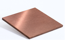
Diamond‑copper composite (DC) is an advanced metal‑matrix composite material consisting of diamond particles as the reinforcement phase and copper as the matrix, fabricated through state‑of‑the‑art composite preparation techniques. Diamond has the highest thermal conductivity of any naturally occurring material, with isotropic values ranging from 1200 to 2300 W/m·K. Copper, with a thermal conductivity of 401 W/m·K, ranks second only to silver among common metals. By combining the two, the compo
-
Mosaic Single‑Crystal Diamond: Breaking Size Limits
With an ultra‑wide bandgap of 5.47 eV, ultra‑high thermal conductivity (>2000 W/m·K), high carrier mobility (electron mobility up to 4500 cm²·V⁻¹·s⁻¹), and ultra‑high theoretical breakdown field strength (>10 MV/cm), Single‑Crystal Diamond (SCD) is an ideal candidate for next‑generation high‑power, high‑frequency and extreme‑environment electronic devices. However, both natural diamond and HPHT‑synthesized single‑crystal diamond are limited in lateral size, which greatly hinders large‑scal