

- 中文
- English
- Español
The surface roughness of diamond single crystal wafers used in High Light Semiconductor can be less than 1nm
2025-03-07 09:48:44
Click:
“
The semiconductor industry is developing rapidly, and breakthroughs in material performance herald a technological revolution. High Light Intelligence Technology, as an outstanding diamond material company, announced that the surface roughness Ra of diamond single crystal wafers has broken through to less than 1nm, and double-sided polishing can be achieved, which will help semiconductor performance breakthroughs.
”
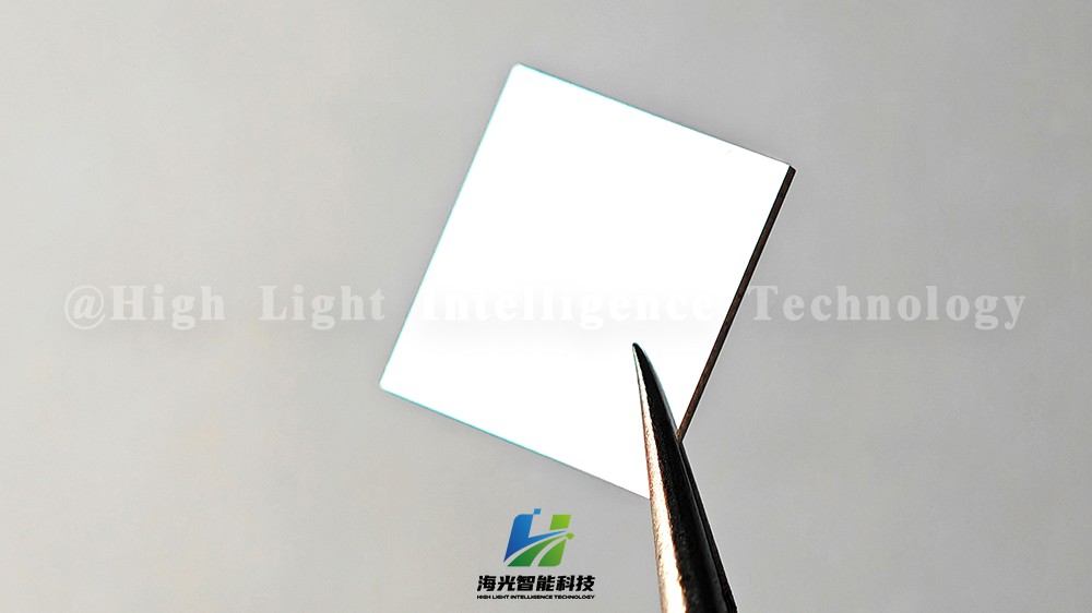
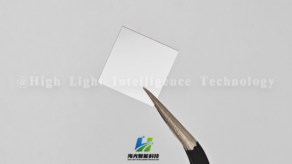
Diamond’s excellent electrical properties enable it to withstand higher frequency currents, making it possible to develop high-frequency devices.
The surface roughness Ra is less than 1nm, which effectively reduces surface defects and improves device performance and reliability.
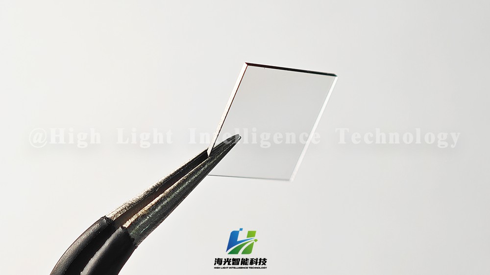
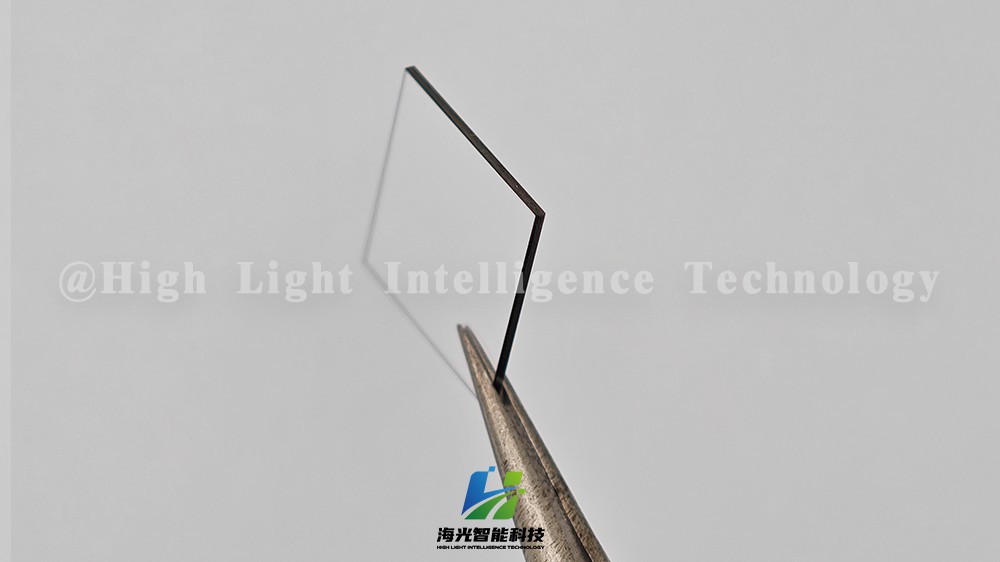
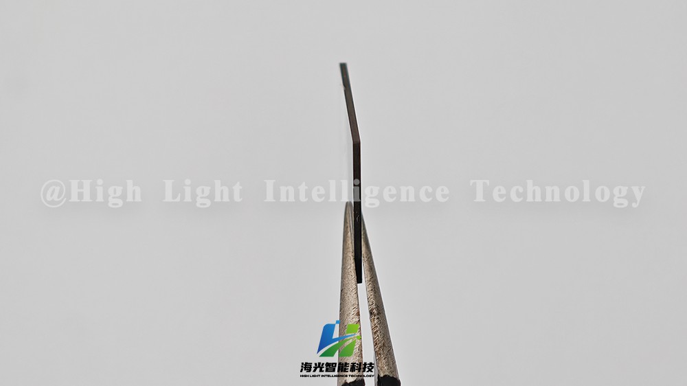
We can provide double-sided polishing services according to customer needs to meet the manufacturing needs of higher precision devices.
The MPCVD technology independently developed by High Light is used to ensure stable and reliable material performance.
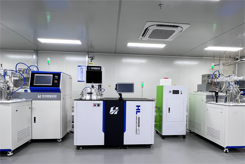
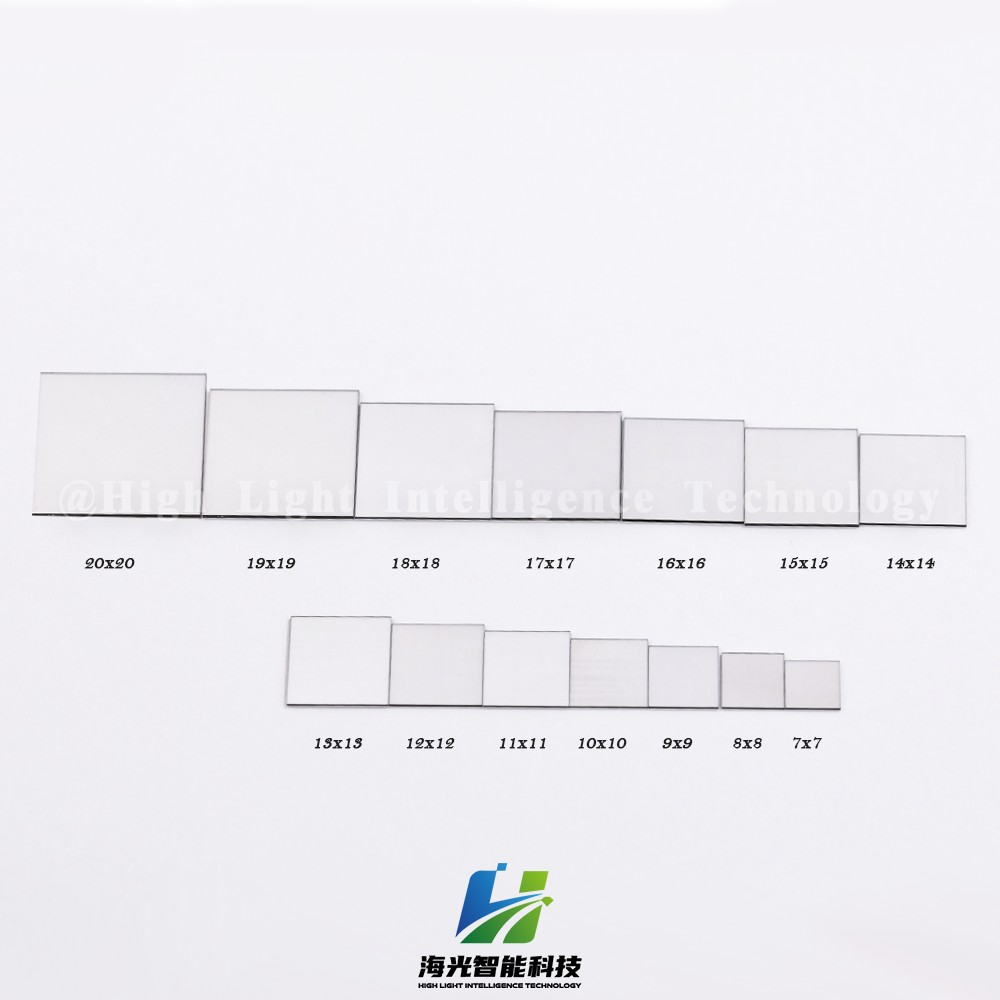
We provide single crystals with sizes ranging from 10x10 to 18x18mm. We can provide diamond single crystals of different sizes and specifications according to customer needs to meet diverse application requirements.
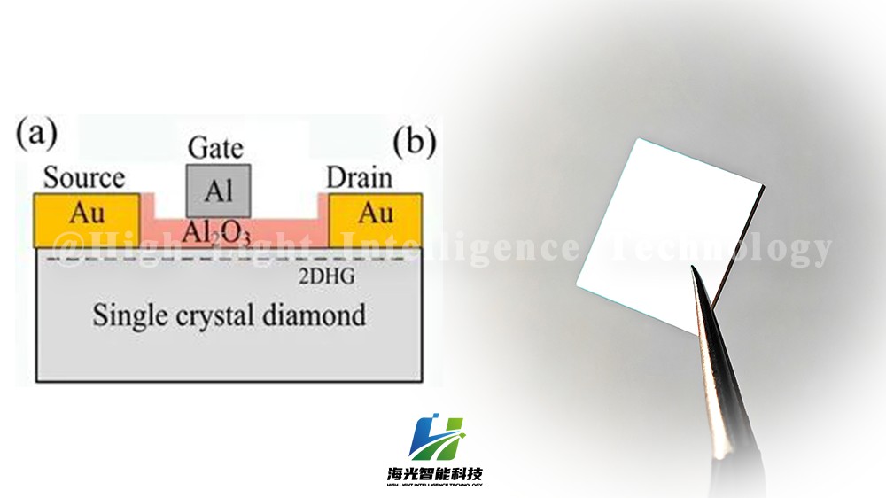
Such as RF devices, microwave devices, etc., helping to achieve higher frequencies and smaller sizes.

Such as pressure sensors, temperature sensors, etc., to improve sensor sensitivity and stability.
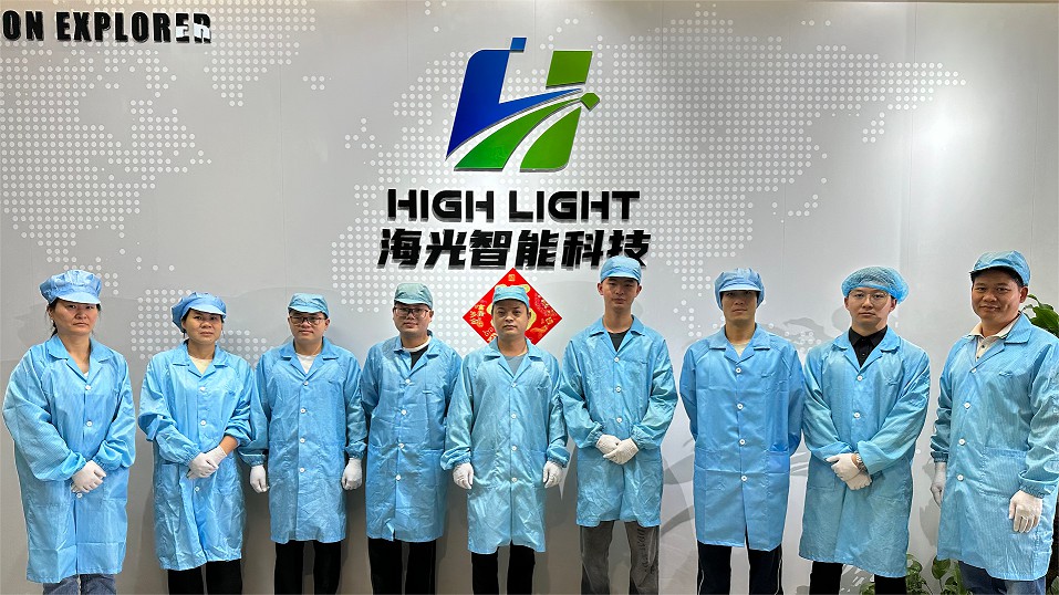
High Light Intelligence Technology, a pioneer in the CVD diamond industry, has advanced MPCVD technology and CVD diamond production workshops. We focus on producing high-purity lab-grown diamonds for the jewelry industry, and at the same time create industrial-grade CVD diamond products, covering single crystals, polycrystalline, films and diamond surface metallization. We also provide 6kw/10kw/15kw MPCVD equipment to help customers in all aspects, from equipment to products, and then to all-round services, to create brilliance together.









-

CVD Single-Crystal Diamonds: An Analysis of the Complete Processing Workflow from Gas-Phase Deposition to Finished Diamond Chips
MPCVD (Microwave Plasma Chemical Vapor Deposition) technology is currently the core process for producing high-quality single-crystal diamond s. Thanks to its advantages of low defect rates, high purity, and controllable large dimensions, it is widely used in fields such as semiconductor heat dissipation, precision optics, and high-end sensors. The final quality of single-crystal diamond s depends on comprehensive process control throughout the entire workflow—from vapor deposition growth to pos
-
Single-Crystal or Polycrystalline Diamond — Which Has Greater Potential?
As diamond continues to enter industries such as semiconductors, thermal management, optics, high-power electronics, and precision machining, the requirements for diamond materials are also evolving.
-
Diamond Polishing and Grinding Processes: Core Challenges and Industry Hurdles
Diamond is often hailed as the “ultimate material” – ranking 10 on the Mohs hardness scale, boasting an ultra‑high thermal conductivity (~2,200 W/(m·K)), excellent chemical stability, and broad optical transparency. These properties make it irreplaceable in cutting‑edge applications such as semiconductor heat dissipation, high‑end optics, and quantum chips. Yet the paradox of “good materials are hard to process” is nowhere more evident than in diamond. From rough grinding for planarization to at
-
Single-Crystal vs Polycrystalline CVD Diamond: Process Difference Lies in Growth Logic, Not Equipment
The process difference between single crystal and polycrystalline CVD diamond lies not in equipment, but in growth logic. Single crystal and polycrystalline CVD diamond are two functional new materials with completely independent growth mechanisms, lattice structures and performance systems. Their process logic, product features and application boundaries diverge fundamentally from the very start of deposition and growth. Comparing or selecting materials without considering their underlying crys




